This thread has been locked.

If you have a related question, please click the "Ask a related question" button in the top right corner. The newly created question will be automatically linked to this question.

ISOW7741DFMEVM: Why is the copper pour under the device cut out?

Part Number: ISOW7741DFMEVM
Other Parts Discussed in Thread: ISOW7741

Hello,

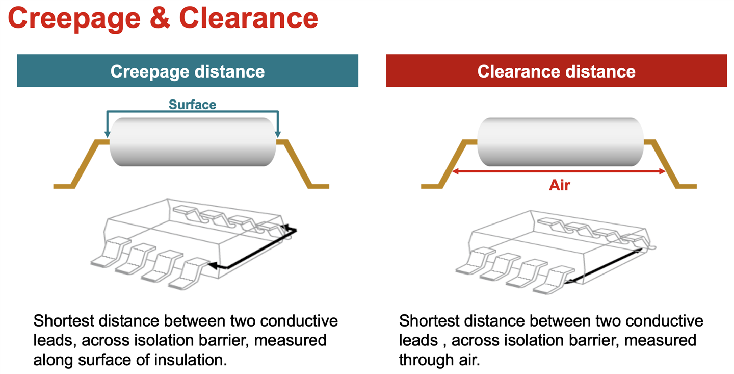
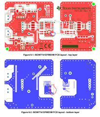
Could someone explain why the polygon under the ISOW7741 is cur out in the EVM? This looks intentional.

Thanks!

John

  • Hi John,

    Thanks for reaching out.

    Yes, the area under the device is intentionally kept free from any copper traces or polygons. This is necessary to maintain isolation ratings and creepage / clearance requirements of the application. If the application doesn't have high isolation requirements then they can relax these requirements and allow traces and polygons underneath the device to the extent that they deem suitable for their application.

    The presence of traces or polygons doesn't affect ISOW7741 operation or performance, this is primarily needed for application isolation requirements. Thanks.

    Let me know if you have any questions, thanks.


    Regards,
    Koteshwar Rao

  • Hi Koteshwar,

    Thanks for the quick response! What confuses me about what you said is that the two ground planes (left and right side of board) above and below the area of the device are closer together than the area under the device. So isn't the limiting factor of the PCB isolation those area of the PCB and not the area under the device? Or, for another example, the exposed copper pads of the footprint of the IC are also closer together. 

    Thanks,

    John

  • Hi John,

    Thanks for seeking clarification.

    It is only the area under the body of device that's critical for determining creepage, clearance and isolation ratings of the solution. Any point from the pads for device pins either side, there is no constraint. Those traces or polygons do not impact the isolation ratings.

    Please see below an image describing creepage and clearance, creepage is measured along the surface and clearance is through air. Introducing traces / polygons under the device can reduce these dimensions. Even traces and polygons underneath device but are on inner layers can impact overall isolation ratings, although lower impact compared to top and bottom layers.

    Let me know if this is clear and answers your question, thanks.


    Regards,
    Koteshwar Rao

  • Thanks, this helps a lot!

    John