This thread has been locked.

If you have a related question, please click the "Ask a related question" button in the top right corner. The newly created question will be automatically linked to this question.

ISO1042DWEVM: ISO1042DWVR

Part Number: ISO1042DWEVM
Other Parts Discussed in Thread: ISO1042, SN74LVC1G17

Hi,

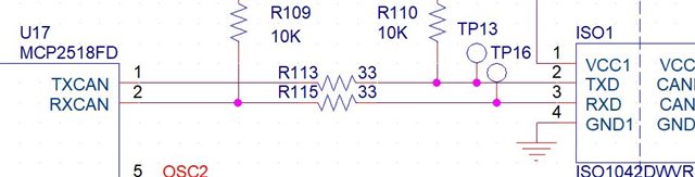
In my design I have the ISO1042DWVR that connects to MCP2518FD with the RX and TX pins (see pictures).

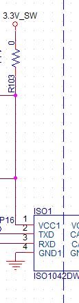
My design is getting the supply from batteries. The VCC1 pin gets 3.3V (with buck power supply from the batteries of 3.3V, and series FET after the buck, then to the VCC1).

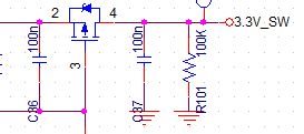
I want that the ISO1042DWVR IC will consume very low current when I do not need to use the communication. So, I added series FET from the 3.3V to VCC1 and I turn on the FET only when I want to communicate (see picture).

from what I understand, when the FET is off then VCC1=0V, and the TX and RX pins can be 3.3V (from the MCP2518FD) and its not allowed to the ISO1042DWVR that TX and RX will be higher than VCC1+0.5V.

When the FET is off there is 100kohm resistor to ground (see picture).


My questions are:

1. Is there another way to set the ISO1042DWVR into sleep mode?

2. Is there a protection diode from TX and RX to VCC1? what is the maximum current allowable of this diode?

3. Is the design looks ok?


PIC 1:

PIC 2:

PIC 3:

Thank you

  • Hi Maor,

    Thank you for your interest in ISO1042. Thank you also for reaching out to seek clarifications on your design. Please see my inputs below,

    from what I understand, when the FET is off then VCC1=0V, and the TX and RX pins can be 3.3V (from the MCP2518FD) and its not allowed to the ISO1042DWVR that TX and RX will be higher than VCC1+0.5V.

    Your understanding is correct, the voltages at TX and RX cannot be more than "VCC1 + 0.5V". If VCC1 = 0V, then TX and RX cannot have anything more than 0.5V.

    1. Is there another way to set the ISO1042DWVR into sleep mode?

    The setup you have used for sleep mode seems good already. To avoid the device getting powered-up through TX and RX, you could probably use a logic buffer with failsfae inputs like SN74LVC1G17. This device can accept input signal voltages upto 6.5V even when its supply voltage is 0V.

    2. Is there a protection diode from TX and RX to VCC1? what is the maximum current allowable of this diode?

    There is an ESD bypass diode placed between TX / RX and supply pin. The diodes are designed to handle HBM ESD pulses only for a few 100ns and hence, do not have a continuous current rating. We also not recommend passing any continuous current through them.

    3. Is the design looks ok?

    The design looks good. I didn't see a 0.1µF cap on VCCx pins. We need a 0.1µF cap on both VCC1 and VCC2 pins, placed as close as possible to device pins. Having an additional 1µF or even 10µF on VCC2 further helps maintain a steady supply for the CAN bus.

    Let me know if you have any questions, thanks.


    Regards,
    Koteshwar Rao

  • Hi,

    Thank you for your answer.

    1. So i must put the SN74LVC1G17? Is it fast enough to handle the communication? Do i need to put it on both RX and TX?

    2. Without the SN74LVC1G17 the ISO1042DWVR will not handle the stress?

    3. Do i need to put pull up resistors?

    Thank you!

  • Hi Maor,

    Thanks for following up.

    1. Yes, they have very low propagation delay and shouldn't have any issues in supporting CAN datarates.
      1. Since you will only be applying an input signal to TX, only this might require a buffer. The RX is an output pin and you can only read voltage from this, hence, a buffer is not needed.
    2. Without SN74LVC1G17, you will be violating the abs max spec of ISO1042. Since there is ESD bypass diode between TX and VCC1, it might accidentally power-up the device when TX is applied while VCC1 is 0V.
    3. Pull-up resistors are not a requirement, having them is also not an issue.


    Regards,
    Koteshwar Rao