This thread has been locked.

If you have a related question, please click the "Ask a related question" button in the top right corner. The newly created question will be automatically linked to this question.

ISO6760: Detail of VIH, VIL, Threshold

Part Number: ISO6760

Hi team,

I would like to ask the device VIH and VIL.

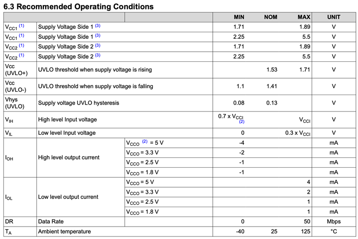
1. Since VIH (min) = 0.7*Vcc, VIL (max) = 0.3*Vcc, VIT+ (max) must be same as VIH (min), VIT- (min) must be same VIL (max). It is obviously, but are all tested?

2. If tested, can we know the distribution of both VIT?

3. VI Hys (min) =0.1*Vcc, it means, if my understanding is correct, there is VIT+ = 0.6*Vcc VIT- = 0.5*Vcc for example. Correct? This can be explained in detail if second question can be known.

4. Customer wonder whether ISO6760 reacts to noise of short period. Does the device have minimum pulse width? This question expects the case of >50MHz (<20ns) noise will cross the thresholds.

If some should be INTERNAL, please email me. I want to left the others public for future reference.

Best regards,

Hayashi

  • Hi Hayashi-san,

    Thanks for reaching out. Please find my inputs below,

    1. Please note that VIH and VIL and recommended voltages. i.e., we recommend customers to apply the input signals in these recommended voltage ranges. While VIT+ and VIT- are the actual device input thresholds. Devices are characterized for VIT± accordingly VIH/VIL recommendations are made.
    2. VIT thresholds are characterized to find out the worst-case spec and accordingly quoted in the datasheet as only they are going to be important for customer to design their systems. e.g., VIT+(max) is 0.7*VCC. This tells customer that they need to apply an input signal that is greater than VIT+(max) for it to be treated as HIGH 100% of the time. It doesn't matter whether VIT+(min) is 0.5*VCC or 0.6*VCC, customer would still have to apply an input signal that is greater than VIT+(max) for it to be treated as HIGH 100% of the time. Hence, only the worst-case specs are quoted in the datasheet.
    3. Your understanding is correct. VI(HYS)(min) of 0.1*VCC means that there will be at least 0.1*VCC difference between VIT+ and VIT- at any given time.
    4. Any noise signal at the input which looks like valid signal, i.e., has voltage levels swinging VIL and VIH levels, then that should be assumed to be treated as a valid signal. If customer expects such noise at input pins then we recommend customer to use necessary input filters.

      I hope this answers all your questions, thanks.


      Regards,
      Koteshwar Rao

    5. Hi Rao,

      Let me follow up the question.

      Could you have data or expectation of distribution of VIH and VIL? Is it a gaussian distribution or is there some other trimming?

      Regards,

      Hayashi

    6. Hi Hayashi-san,

      Thanks for the follow-up question.

      VIH and VIL are not device specifications, rather they are the input voltages that we recommend you to apply to device input pins for it to accept them as valid HIGH and LOW signals, respectively. e.g., The recommended VCC voltage range is 1.71V to 5.5V (as shown in below table), this is the voltage that we recommend you to apply and there is no distribution associated with it. It is the same for VIH and VIL as well, these are recommendations.

      The VIT+ and VIT- are device thresholds and they follow Gaussian distribution. I believe this is what you wanted to know, thanks.

      Regards,
      Koteshwar Rao