A related question is a question created from another question. When the related question is created, it will be automatically linked to the original question.
If you have a related question, please click the "Ask a related question" button in the top right corner. The newly created question will be automatically linked to this question.
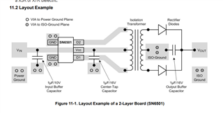
Yes, it is certainly better to keep the current loop directly to the device as short as possible. In the example layout diagram, all the GND points are suggested to be connected to a GND plane which is a best to keep the current loop as short as possible.
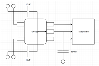
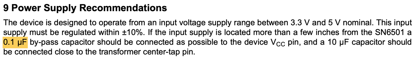
Yes, although it is not shown in the layout diagram, an additional cap of 0.1µF is recommended to be connected to VCC pin. Please see below snapshot from datasheet, thanks.
In terms of emissions, wouldn't it be better to connect the capacitors to the IC ground directly in the TOP layer instead and then using vias instead of using vias directly to the ground plane? I would understand that connecting directly would have less inductance in the return path between the IC and the capacitor
Your understanding is correct, a direct connection helps in many ways including keeping switching noise to minimal. Even in the example layout they are connected directly and to the GND plane as well. I am sorry it is not explicitly mentioned, but they are indeed connected on the same plane and also connected to a GND layer on a different plane and this is the recommendation.
Let me know if this answers your question, thanks.