A related question is a question created from another question. When the related question is created, it will be automatically linked to the original question.
If you have a related question, please click the "Ask a related question" button in the top right corner. The newly created question will be automatically linked to this question.
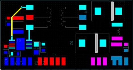
The vias going to add some inductance and cause some ringing in the switching waveform, leading higher emissions and/or lower efficiency. Although it might not be a major concern, it is recommended to run both the SW1 and SW2 nodes on the top layer with shortest possible trace between SN6507 and the transformer.
Let me know if you have any further questions, thanks.