This thread has been locked.

If you have a related question, please click the "Ask a related question" button in the top right corner. The newly created question will be automatically linked to this question.

SN6501-Q1: Static current deviation phenomenon

Part Number: SN6501-Q1
Other Parts Discussed in Thread: SN6501

Hi Office,

Good Day!

I have used SN6501 in my isolated part. When the product is manufactured, there is a current deviation issue happened in some cases.

I set an EOL spec as 65-80 mA for static current. But it has a current deviation, generally up or down by 10mA.
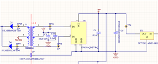
Here are the actions I took:

1. Replace U1 SN6501 with a new one, and it goes back to normal.

2. Change the U1 on the high one with the low one, and both of them go back to normal.

3. Resolder the U1 and change nothing, and it keeps high/low bias.
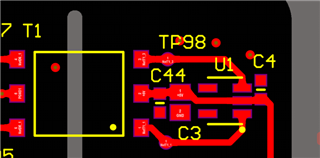
I wonder why there is a static current deviation.
1. Cause by my layout design?
2. Cause by my stray capacitance?

Thanks in advance!

  • Hi Hang,

    Welcome to TI E2E Forum!
    Thank you for reaching out and sharing details related to your question.

    I may not have understood your issue completely but please allow me to describe what I have understand from your post and seek clarification.

    1. You are using SN6501 to generated an isolated 5V output from 5V input supply.
    2. The load connected to the isolated 5V is between 65-80mA?
    3. When a given load is connected at the output, the input supply current to SN6501 either increases or decreases by upto 10mA?

    Could you please confirm if my understanding is correct? If it is not, could you please correct me and elaborate about the issue you are facing?

    I have reviewed the schematic and PCB layout and they both look good. I do not expect any major issues due to the schematic and PCB layout. It would help me understand the issue better if you could elaborate about the issue. Thanks.


    Regards,
    Koteshwar Rao

  • Hi Koteshwar,

    Sorry for my error of expression.

    You are using SN6501 to generated an isolated 5V output from 5V input supply.

    This is correct.

    • The load connected to the isolated 5V is between 65-80mA?
    • When a given load is connected at the output, the input supply current to SN6501 either increases or decreases by upto 10mA?

    In fact, the product is divided into two parts, High Voltage and Low Voltage.

    The “isolated 5V" is the supply power for op-amp sampling. And I have two isolation loops.

    The "65-80mA" current is the Low Voltage load current, measured by floating High Voltage part.

    And the current bias, which either increases or decreases by upto 10mA, sometimes happened on the measurement.

    I think it means that something is affecting my circuit, changing the static load current.

    And below are some actions I have tried.

    1. Replace U1 SN6501 with a new one, and it goes back to normal.

    2. Change the U1 on the high one with the low one, and both of them go back to normal.

    3. Resolder the U1 and change nothing, and it keeps high/low bias.

    If anything is unclear, please point it out. Thanks!

    Regards,

    Hang An

  • Hi Hang,

    Thank you for sharing additional information, I think I understand a little more now. To make sure I have understood it correctly, please allow me to share what I have understood and seek further clarification.

    1. The outputs VDD1_5V and VDD2_5V are powering two separate Op-Amp circuits.
    2. The total load connected to VDD2_5V is about 65-80mA.
    3. The Op-Amp connected to VDD1_5V monitors the load current on VDD2_5V and is measured and converted to digital by an ADC in an MCU.
    4. This measured current has an error of ±10mA compared to the actual load current on VDD2_5V.

    Please help confirm if my understanding is correct.

    Please note that I can only see the schematic that you have shared and I can only understand from what you share. To resolve the issue faster, it would help if you could share all information related to the issue. I am listing below some of the information that might help.

    1. Where is 65-80mA observed?
      1. Please confirm this explicitly like is it the current on VDD1_5V, VDD2_5V, +5V or any other node in the schematic.
    2. How or where is the current measurement being done?
      1. Confirm which current and share relevant schematic to review.
      2. If possible, please share complete schematic so that I understand the overall connections.
    3. Is the 10mA increase or decrease a measurement error or is it an actually current on some node being higher or lower?
      1. Please be as specific as possible.
      2. If it was measurement error, please note that there are many components involved that could affect the measurement error. Hence, a complete schematic and a more specific description would help resolve issue faster.
    4. Please share any other information that might help me understand the issue better.


    Regards,
    Koteshwar Rao

  • Hi  Koteshwar,

    Sorry for the delay for personal reasons.

    The outputs VDD1_5V and VDD2_5V are powering two separate Op-Amp circuits.

     1. Correct. The outputs are powering two separate Op-Amp circuits.

    The Op-Amp connected to VDD1_5V monitors the load current on VDD2_5V and is measured and converted to digital by an ADC in an MCU.

     2. The load current is for the whole product, including VDD1_5V and VDD2_5V.

    This measured current has an error of ±10mA compared to the actual load current on VDD2_5V.

    3. The two Op-Amp circuits have no relation. They are similar in measuring different part currents.

    The total load connected to VDD2_5V is about 65-80mA.

    4. This measured current has an error of ±10mA compared to the actual load current on the product.

    In the beginning, all my current measurements were based on the entire product. Later, I did some tests, including replacing the new SN6501 chip and exchanging the chips on products with high and low currents.

    • Where is 65-80mA observed?
      1. Please confirm this explicitly like is it the current on VDD1_5V, VDD2_5V, +5V or any other node in the schematic.
    • How or where is the current measurement being done?
      1. Confirm which current and share relevant schematic to review.
      2. If possible, please share complete schematic so that I understand the overall connections.
    • Is the 10mA increase or decrease a measurement error or is it an actually current on some node being higher or lower?
      1. Please be as specific as possible.
      2. If it was measurement error, please note that there are many components involved that could affect the measurement error. Hence, a complete schematic and a more specific description would help resolve issue faster.
    • Please share any other information that might help me understand the issue better.

    The current measurement is measured at the power supply end to get 65-80mA. I observed the current on Vpower and GND.

    I don't think it was a measurement error because I have a pile of defective products piling up.

    When I cut copper and disconnected U1, and only U4 worked, the current deviation still existed, but it became half of what it was before. For example, when I removed the U1 circuit from two products with high current (90mA) and low current (60mA), 90 became 53, 60 became 37, and the overall deviation changed from 90-60=30 to 53- 37=15.
    Combined with the results of my exchange of U1 at the beginning: when I exchange U1 with two products with high current (90mA) and low current (60mA), the current returns to the normal range (75mA).

    It looks weird. It seems like every one of my circuits is going off. And the final 10mA error is just a permutation of each small deviation.

    Hoping my information will help. Thanks in advance!

    Regard,

    Hang An

  • Hi Hang,

    Thanks for your inputs, please allow me to review the information you have shared and come back to you with my inputs. Thanks.


    Regards,
    Koteshwar Rao

  • Hi Hang,

    Thank you for your patience and for sharing additional information including the larger schematic.

    From the shared schematic, I now understand that the current being monitored is from a different source and not related to the load on SN6505. To interpret the schematic better and understand what all components could be contributing, could you pleas share the schematic in PDF? The attached schematic picture is blurry and I am unable to read any text in the schematic. Thanks.


    Regards,
    Koteshwar Rao

  • Hi Hang,

    Thanks again for sharing the schematic in PDF which I was able to read clearly and understand how SN6501 is used in your application.

    I am assuming the solution is an Insulation Monitor where current of two different resistor dividers are buffered, isolated and then converted to digital either using external ADC or with ADC integrated in MCU. If I understand your original question correctly, the current that you are measuring is off by ±10mA and it gets corrected if you replace the SN6501 device. Please confirm if my understanding is correct.

    Could you please mention replacing which of the two devices (U1 or U4) fixes the issue?

    Could you please also monitor the output voltage at nodes TP3, TP18, VDD1_5V and VDD2_5V when the board is showing current reading off by ±10mA?
    The only way SN6501 can impact the measurement is by its output voltage and monitoring this voltage under normal and fault conditions will let us know what the issue could be. Let me know, thanks.


    Regards,
    Koteshwar Rao

  • Hi Koteshwar,

    When I replace the SN6501 with a new one, the current gets corrected. I can confirm it works for both U1 and U2.

    Could you please also monitor the output voltage at nodes TP3, TP18, VDD1_5V and VDD2_5V when the board is showing current reading off by ±10mA?

    This is the output voltage:

    For total lower one:

    TP3=6.246V TP8=VDD1_5V=4.988V    TP15=6.274V TP25=VDD2_5V=4.984V

    For total higher one:

    TP3=6.373V TP8=VDD1_5V=4.991V    TP15=6.380V TP25=VDD2_5V=5.002V

    For lower without U1 circuit (without VDD1_5V):

    TP15=6.265V    TP25=VDD2_5V=4.984V

    For higher without U1 circuit (without VDD1_5V):

    TP15=6.412V    TP25=VDD2_5V=5.008V

    Seems the higher products have higher VDDx_5V.

    I think I found why, the deviation may be caused by the operation of the isolation op amp SI8920 at the next stage.

    Could you help confirm my suppose?

    Thanks,

    Hang An

  • Hi Hang,

    Thanks for your inputs, this is useful.

    When I replace the SN6501 with a new one, the current gets corrected. I can confirm it works for both U1 and U2.

    Could you please clarify replacing which device resolves the issue as also requested earlier? Is it U1, U2 or both?

    For total lower one:

    TP3=6.246V TP8=VDD1_5V=4.988V    TP15=6.274V TP25=VDD2_5V=4.984V

    For total higher one:

    TP3=6.373V TP8=VDD1_5V=4.991V    TP15=6.380V TP25=VDD2_5V=5.002V

    It looks like the SN6501 outputs are fine although there is voltage differences, I believe that is small enough not cause any major concerns. When you refer to TP15, I am assuming that you are referring to TP18 in the schematic that you shared in previous posts.

    I am also not clear what you mean by lower and higher here. Do you have two sets of circuits with each one consisting of two SN6501?

    For lower without U1 circuit (without VDD1_5V):

    TP15=6.265V    TP25=VDD2_5V=4.984V

    For higher without U1 circuit (without VDD1_5V):

    TP15=6.412V    TP25=VDD2_5V=5.008V

    Based on your description, it looks there are two sets of circuits with each containing two SN6501 devices and you testing with U1 removed in both circuits.

    Seems the higher products have higher VDDx_5V.

    They seem marginally higher but that is an outcome of the LDO NCV551 which should produce an output according to your needs. If they don't then you choose the LDO meets your requirements. SN6501 cannot regulate its outputs and hence, SN6501 doesn't determine your circuit performance.

    I do understand that replacing SN6501 is also resolving the issue. This only indicates that the LDO output regulation might not be meeting your requirement and might need a device with better accuracy and PSRR. You might want to reach out to LDO manufacturer to understand what voltage accuracy and PSRR are needed on their VDD pins to produce signal that meets your requirements. Based on this, you can choose the LDO that meets the specified accuracy and PSRR.

    All this information points out that SN6501 isn't the cause of the issue although changing this device is indirectly helping resolve the issue. This is not because SN6501 output was bad but maybe because the post-regulator LDO output is too dependent on its input.

    If everything is clear, I would like to go ahead and mark this thread as closed. Let me know, thanks.


    Regards,
    Koteshwar Rao