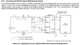
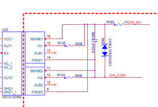
This thread has been locked.

If you have a related question, please click the "Ask a related question" button in the top right corner. The newly created question will be automatically linked to this question.

ISO1212: ISO1212DBQ_Ground reference clarification

Part Number: ISO1212

Hi Team,

I have below circuit in one of the design and currently we are working on the layout, We used 10layer stack up for this and first 2layer structure is as below.

We have routed DIN_IN1 and DIN_COM1 on the top and layer. What should be the reference layer on the GND1 plane for these two signals?

Top

GND1

Regards,

Chitharanjan M

  • Hello Chitharanjan,

    Thank you for reaching out. It looks like channel 2 is unused and grounded, this is fine. One quick comment on your schematic. SUB1 and SUB2 need to be connected to small 2mm x 2mm floating plane for thermal performance. 

    Otherwise FGND1 and FGND2 can be connected together and referenced to their own ground plane. They should not connect to GND1.

    Best,
    Andrew

  • Hi Adrew,

    Here both the channels were used in Current sink and source configuration as per below application schematic from the datasheet.

    Since both the grounds are separated by CIN capacitor which ground reference should be provided in the second layer of the PCB.?

    One quick comment on your schematic. SUB1 and SUB2 need to be connected to small 2mm x 2mm floating plane for thermal performance

    We have taken care this.

    Regards,

    Chitharanjan M

  • Hello Chitharanjan, 

    Thank you for the clarification. The application for ISO1212 will differ from other logic circuits. The diagram shown in figure 28 has each of the input pins (INx and FGNDx) connected to the same sensor. However, input 1 is connected as a sourcing type input and input 2 is a sinking type. For this reason, the diagram shows an "IN" terminal and a "COM" terminal instead of a typical GND for the sensor.

    The input should be provided with the same ground reference as the field sensor. In your schematic DIN_IN1 and DIN_COM would be connected to the field sensor's IN and COM terminals respectively. This would likely make the COM the best ground reference for your PCB.  

    Best,
    Andrew

  • This would likely make the COM the best ground reference for your PCB.

    Thanks for the clarification, we will make COM as ground reference