This thread has been locked.

If you have a related question, please click the "Ask a related question" button in the top right corner. The newly created question will be automatically linked to this question.

ISO7741: PCB layout differences between IOSxxx and ADuMxxxx

Part Number: ISO7741

Hi toghter,

In the TI Digital Isolator Design Guide SLLA284G it is mentioned to keep the space under the ISOxxxx component free of planes, traces, pads and vias.

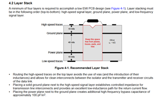
In comparison, the application note AN-1109 of Analog Devices, a guideline for PCB layouts of digital isolators (ADuM series) recommends to build an overlapping stichting capacitor beneath the isolator.

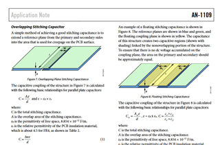
Can somebody explain, why the recommendations are so different for the ground plane design for digital isolators of TI and Analog Devices? Is it caused by the coupling technology? ISOxxx isolators use a capacitive coupling. In comparision, The ADuMxxxx isolators use a magnetic coupling.

Thanks a lot for your answer and explanation.

Best regard,

Basil

  • Hello,

    Thank you for your question. 

    Please give us an additional day to review your question and respond.

    Regards,
    Aaditya Vittal

  • Hi Basil, 

    Thank you for your questions and for your patience.

    For digital isolator devices, we recommend to keep the space under the isolator free of traces, planes, etc. so that the device can meet the creepage/clearance and isolation requirements.

    From the document you provided, it seems that the stitching capacitor is a special case and may be included as a larger section in order to address specific EMC challenges.

    Generally speaking, the stitching capacitor helps improve EMC issues. This method can also be used for TI digital isolators to help with EMC challenges, but it is not required for the operation of the device. One thing to note is that the stitching capacitor significantly decreases the isolation rating for the overall system/solution.

    Regards,
    Aaditya Vittal

  • Hi Aaditya,

    Thanks for your response. So, it is not strictly dependent from the coupling technology (capacitive or magnetic) which PCB design for the GND planes should be used. 

    Best regards, 

    Basil