Other Parts Discussed in Thread: ISO7740, , ISO7240CF
Tool/software:
Dear Technical Support Team,
Unexpected momentarily glitch(about 2.5V , 8us) on the output during power up, at a time when Vcc2 is at about 2.5V.
See attached file.
Q1
Do you have any work around to avoid glitch?
Q2
What root cause does this problem?
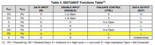
Since glitche occurs around Vcc2=2.5V, I assume that the output circuit at that time may still be indeterminate and is High.
(Operation is guaranteed at Vcc2=3.16V or higher.)
Q3.
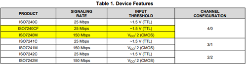
How about ISO7740(OOK) to avoid problem? ISO7240M is edge-based.
【Conditions】
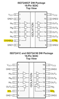
・ISO7240MDW
・Vcc2 (5V) power up about 2.5ms after Vcc1 (3.3V) power up at first.
・LOW level voltage is already applied to the Input pin.
・Enable pin is connected to the 5V power supply.
・There is no pull-up resistor on Output pin.

Best Regards,
ttd