This thread has been locked.

If you have a related question, please click the "Ask a related question" button in the top right corner. The newly created question will be automatically linked to this question.

SN6507: The SN6507 does not work with Wide-Ranging Input with Duty Cycle Control

Part Number: SN6507

Tool/software:

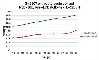
I can't start operation of the SN6507 with enabled duty cycle control.

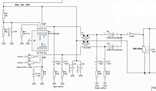
Can you please provide the application schematic for SN6507 operating with Wide-Ranging Input voltages with Duty Cycle Control which includes names of all compnents? The best for me when it includes Transformer WE 750319693. 

My application requirements: Vin min = 16V, Vin max = 27V, Vout = 27V, Iout = 0.2A. But any schematic that works would be helpful to me.

Thank you,

Darek

  • Hi Darek,

    Welcome to TI E2E forum!

    Thank you for reaching out and sorry to hear that your design is not working. The application schematic of SN6507 with duty cycle control enabled is provided in Figure 8-3 and Figure 9-4 of SN6507 datasheet, I am copying below Figure 9-4.

    You can also find a detailed schematic with component values in EVM schematic. I am copying below the direct link of EVM for SN6507. On this page, you will find EVM user's guide which includes EVM schematic, PCB layout and BOM, among other things.

    https://www.ti.com/tool/SN6507DGQEVM

    Please share your schematic so that I can review and confirm if there are any concerns in the design, thanks.


    Regards,
    Koteshwar Rao

  • Dear Koteshwar,

    Thank you for the quick reply. First I tried with the schematic below:

    To sum up: Rdc=33k, Rsr=NC, Rclk=10k, Rlim=22k, Tr 1:2.29, L=220uH

    Then I tried with DevKit with similar settings, but L=33uH (included in the DevKIT). I did tests for Rclk=10k and Rclk=4.7k and for tr 1:0.71 (as it is originally in DevKIT) and with tr reversed so tr 1:1.4

    I have not been able to reduce the duty cycle.

    My application requirements: Vin min = 16V, Vin max = 27V, Vout = 27V, Iout = 0.2A. This is power supply of IGBT driver so the current will be sourced only when the transistor will be switched. In the idle mode I<10mA

    Darek

  • Hi Dariusz,

    Thank you for sharing the schematic and additional details. Please allow me to review this information and come back to you tomorrow, thanks.


    Regards,
    Koteshwar Rao

  • Dear Koteshwar,

    Thank you. I look forward to your suggestions.

    KR, Dariusz

  • Hi Dariusz,

    Please allow Koteshwar and additional day to review and reply. Thank you for your patience.


    Regards,

    Aaditya Vittal

  • Hi Dariusz,

    Thank you for your patience.

    For your application input / output voltage requirements and with the schematic with RDC = 33kΩ, the typical duty cycle is calculated to be 18%. This should be designed at 25% so that the variation in input doesn't exceed the allowable duty cycle range. To achieve 25% duty cycle, I recommend using RDC = 46kΩ with everything else remaining the same.

    For testing purposes, I suggest a minimum load of 20mA if LMIN=220µH or 130mA if LMIN = 33µH.

    Please do test with the suggested RDC and LMIN and let us know the results. Thanks.


    Regards,
    Koteshwar Rao

  • Dear Koteshwar,

    Thank you, I will do the tests and get back to you with the results.

    In the meantime, can you share with me information how did you calculated Rdc?

    In my calculations, I used equation no. 1 on page 13 from the datasheet with parameters D = 0.25, VCC = 16, Rclk = 9.6 and the result was Rdc = 33.6k

    Kind regards,

    Dariusz

  • Hi Dariusz,

    I believe the difference in your and my calculations is due to VCC value. VCC in Equation (1) should be nominal input, the center value of input voltage range. In your application, it is 21.5V (I used 22V for calculation) which is in the middle of 16V and 27V. When input is at 21.5V, the duty cycle is going to be 25%. If input voltage increases, the duty cycle decrease and similarly, if input voltage decreases, the duty cycle increases thereby achieving line regulation.

    It is also important that you have LMIN to support the minimum load requirement. A lower minimum load current would require higher inductor value while a higher minimum load can accept a lower inductor value.

    Please do test this and let us know if you still see issues, thanks.


    Regards,
    Koteshwar Rao

  • Dear Koteshwar,

    Thanks for your support. SN6507 works in my application for Rdc ranging from 44.8k up to 68k, figure attached below.


    This resolve my issue.

    Kind regards,
    Dariusz