This thread has been locked.

If you have a related question, please click the "Ask a related question" button in the top right corner. The newly created question will be automatically linked to this question.

SN6505B-Q1: SN6505BDBVR transformer driver based power supply fail in conducted emission test

Part Number: SN6505B-Q1
Other Parts Discussed in Thread: SN6505B

Tool/software:

Dear Sir,

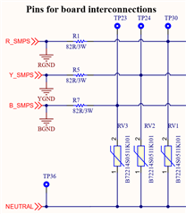
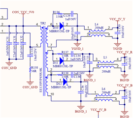
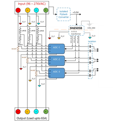
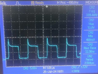
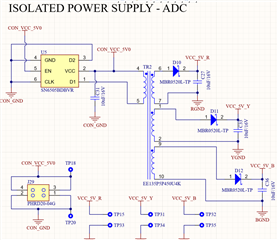
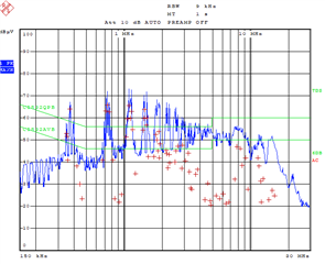
SN6505BDBVR is used in our design in flyback mode to generate the 3 power supplies for the ADC of the 3-phase smart meter. During the conducted Emission test as per the CISPR 32: 2015 standard, it fails at multiple frequencies as shown in the below image. We have also tried several combinations of the snubber circuit on the primary and secondary sides of the transformer according to https://www.ti.com/lit/pdf/SLLA566 but we are still unable to improve the results. Please provide your valuable input to resolve the same as soon as possible. Let me know if you need more information.

Regards,

Nilesh

  • Hi Nilesh,

    Thank you for reaching out and for sharing schematic and conducted emissions plot.

    Since the SN6505B is a push-pull transformer driver, it doesn't have any features of a Flyback converter especially the ones that might help for better EMI and therefore, might not have the best emissions. When the device is used as a push-pull converter, we expect the device to meet CISPR 32 requirements.

    If it is an option to update your design to push-pull topology, please do consider making the changes. If it is not an option then the best way to address conducted emissions is to use EMI filtering on the input supply, assuming you are conducting emissions measurement on the input supply. The filtering can be done using either ferrite beads or common-mode chokes (CMC), the latter are going to be most effective.

    The suggesting providing in the App Note that you have referenced are more suitable for radiated emissions due to ringing on switching waveform but they should also help conducted emissions to some extent. Let me know if you have any other questions, thanks.


    Regards,
    Koteshwar Rao

  • Hi Koteshwar,

    Thanks for your valuable feedback. Please note that our testing of the Conducted Emission is on the secondary side of the transformer. RGND, YGND, and BGND are the 3-phase of the system and conduct the measurement to the neutral terminal in the design. The shared test results are between the RGND (R-Phase) and the neutral and observed the same in the remaining phases. Please provide your suggestions to improve the same.

  • Hi, 

    Thank you for your inquiry.

    Please allow us an additional day to review and get back to you.

    Regards,
    Aaditya Vittal

  • Hi Nilesh,

    Thank you for clarifying and providing additional information.

    I consider that RVCC, YVCC and BVCC are the 3-phases of a system where all the 3 GNDs are shorted to create neutral node. But I am not sure how RGND, YGND and BGND are the phases. If you further schematic showing how these GNDs and VCCs are connected to a 3-phase system and how neutral is created, that would help me understand the implementation and I will be able to better comment on suppressing emissions.

    You can still suppress the emissions by employing EMI filtering on each of the 3 outputs individually, with respect to their own GNDs. Thanks.


    Regards,
    Koteshwar Rao

  • Hi Koteshwar, 

    Please note that RGND is connected to the R-Phase, YGND to the Y-Phase, and BGND to the B-Phase of the 3-Phase Meter directly. VCC_5V_R is a power supply for R-Phase ADC and VCC_5V_Y and VCC_5V_B for Y-Phase and B-Phase ADC respectively. SN6505B generates an isolated power supply for 3 separate ADCs operating voltage.

    AC input voltage and respective phases ground connections, DC voltage CON_VCC_5V0 generated using isolated flyback converter.

    We have tried with multiple EMI filtering circuits in the design as shown below but are still not able to get successful to resolve it. 

    R-Phase ADC measurement circuit.

    Please Let me know if you need more clarification to provide your valuable suggestions to resolve the same.

  • Hi Nilesh,

    Thank you for sharing additional details, this is helpful.

    Could you please help me with the part number of common-mode choke (CMC) used at the supply outputs? I need to see the impedance vs frequency plot to understand its effectiveness in suppressing emissions.

    Please also help me with a picture of test setup showing PCB and connections where emissions are being tapped. Thanks.


    Regards,
    Koteshwar Rao

  • Hi Koteshwar,

    Refer to the below link for the CMC part used in our design and provide your input.

    https://www.we-online.com/components/products/datasheet/784234201.pdf

    The picture of the test setup is not readily available now so refer to the below diagram shows the measurement points for the conducted Emission Test.
    L1 IN -> N
    L2 IN -> N
    L3 IN -> N

    The grounds of each ADC are connected to the respective phase terminal as shown above. Small and Large are resistor dividers for voltage measurement.

    Let me know if you need more information.

  • Hi Nilesh,

    Thank you for sharing the block diagram connection between SN6505B, ADCs and the line voltages, this helps me understand the power supply connections better and now, I don't have any concerns in the connections between SN6505B and line voltages.

    The CMC that you are currently using seems to offer the best attenuation (>10kΩ) between 10MHz and 100MHz while the emissions that you are observing lie between 200kHz and 5MHz. Therefore, I suggest using a CMC that offers the best attenuation in the frequency of interest. This should suppress all the noise and improve conducted emissions results.

    To further review to find any other issues, please help me with the following information.

    1. D1/D2 waveform with respect to respective GNDs.
    2. Output ripple waveform at VCC_5V outputs.
    3. PCB layout of SN6505B and the CMCs to make sure they are positioned to avoid any noise cross-couplings.

    Sorry for asking information repeatedly, everything we have reviewed looked good except for the CMC. Therefore, I am asking for more information to review and identify all other possible issues. Thanks.


    Regards,
    Koteshwar Rao

  • Hi Koteshwar,

    See below the requested information and provide your valuable input.

    1. Waveform at D1 pin. The D2 pin is grounded so not capture waveform.

    2. Ripple voltage at VCC_5V of R, Y, and B secondary respectively.

    Ripple at C27 (VCC-5V-R)

    Ripple at C33 (VCC-5V-Y)

    Ripple at C36 (VCC-5V-B)

    3. ADC PCB layout

    ADC PCB Layout.pdf


    Please review and provide your further input to move forward accordingly.

    Regards,

    Nilesh

  • Hi Nilesh,

    Thank you for providing requested information.

    1. The waveform observed at D1 seems to have quite some overshoot. I am not an expert in Flyback topology, but I found that there RC snubbers or voltage clamps used across transformer to snub/suppress this overshoot. Please see below article for more details. This should help minimize the emissions considerably.

    You can find many more documents on ti.com for general design guidelines on Flyback topology.

    https://www.ti.com/document-viewer/lit/html/SSZTCV6

    2. The output ripple voltage doesn't look like too much.

    3. The PCB layout mostly looks good. Can you please change the value of C31 from 1nF to 0.1µF? We typically recommend 0.1µF cap for VCC of SN6505 and 10µF to the transformer input.

    With the above suggested changes including the change for CMC, I believe the emissions results should improve. Thanks.


    Regards,
    Koteshwar Rao