This thread has been locked.

If you have a related question, please click the "Ask a related question" button in the top right corner. The newly created question will be automatically linked to this question.

ISO7340-Q1: Clarification On ISO7340-Q1 Operating and failure conditions

Part Number: ISO7340-Q1
Other Parts Discussed in Thread: TMS320F28379D

Tool/software:

Dear TI team,

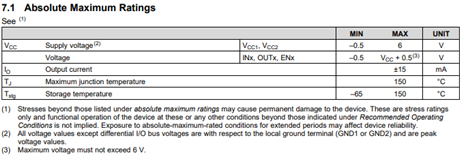
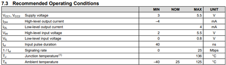
I have a few questions regarding the working and failure conditions of the ISO7340-Q1 high state isolator. The supply voltages are Vcc1 at 3.3V and Vcc2 at 5.3V. The Vcc1 digital pins are connected to the TMS320F28379D GPIO pins, while the Vcc2 digital pins are connected to the Cryton MD20A  board.

If I apply 2.5V to pin 13 and 0.75V to pin 11 while maintaining 3.3V at pins 4 and 6 (which are input pins), what effects can I expect?

Similarly, if I apply 2.5V to pin 13 and 0.75V to pin 11 while pin 4 and pin 6 are at 0V, what will be the outcome?

attached images for your reference 

Thank you for your assistance!

  • Hello,

    Please give an additional day to review and respond.

    Regards,
    Aaditya Vittal

  • Hello,

    Thank you for your patience.

    If I apply 2.5V to pin 13 and 0.75V to pin 11 while maintaining 3.3V at pins 4 and 6 (which are input pins), what effects can I expect?
    Similarly, if I apply 2.5V to pin 13 and 0.75V to pin 11 while pin 4 and pin 6 are at 0V, what will be the outcome?

    Pin 13 and Pin 11 are both output pins. Although the device OUTx pins can tolerate up to 6V (as per absolute maximum ratings), these conditions where a voltage is applied to the OUTx pins is not recommended. We do not guarantee normal operation of the device under these conditions.

    More details on the reason or applications may help us better in explaining the conditions you have asked for, but generally we do not recommend as mentioned before.

    Regards,
    Aaditya Vittal