This thread has been locked.

If you have a related question, please click the "Ask a related question" button in the top right corner. The newly created question will be automatically linked to this question.

SN6507DGQEVM: Latched, recoverable only by input power cycle

Part Number: SN6507DGQEVM
Other Parts Discussed in Thread: SN6507

Tool/software:

Hello TI, 

we are facing issue with SN6507 push-pull transformer driver which is in our power converter supplying IGBT gate driver via transformer - please see attached schematic .

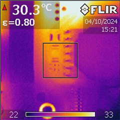
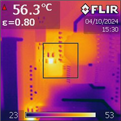
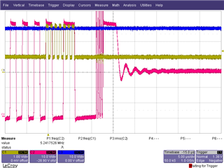
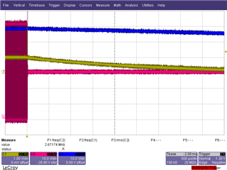
Multiple of SN6507 are operating normally (usually) in our system. With certain pulse pattern in high power electronics circuit, we are facing latching behavior of SN6507, which is not explainable by the datasheet.  Latched mode is permanent, practically up to next power cycle of the input voltage. After cycling the input power, SN6507 continues operating normally, no degradation of performance. During the latched condition, steady voltage on SW1&SW2 (no switching). IC goes to complete idle condition, input voltage is 29,8V. 

By comparing the voltages on pins before and after the event causing the latched mode, we see that CLK voltage drops to 0V. At normal operation, it is typically around 0,98V. Voltages on other pins in latched condition, seem to make sense - PIN4 FB 6.8V (29.8Vin), PIN6 SR 1.132V. 

There might be a short glitch, voltage induced in CLK pin loop, from power electronics circuit which might result in voltage on CLK pin above 1.6V, but this shall not create a permanent latch of the IC, at least not according to the datasheet. 

Can you please suggest what might be the root cause of this behavior and how to avoid it? Is the filter capacitor (e.g. 100nF) on CLK signal acceptable (no influence in normal operation)?

Thank you very much, 

Best Regards,

Michal

  • Hello Michal,

    Thank you for reaching out. There are a few cases that could cause the SN6507 to stop switching. The easiest to check would be to find the VT-product in the manufacture's datasheet and confirm it meets the equations in 9.2.2.5.1 V-t Product Calculation. The transformer needs to have enough margin to ensure that it does not become saturated by the SN6507 switching. Saturation could lead to the solution overheating and cause the SN6507 to enter thermal shutdown or over current protection which would stop switching. 

    Feel free to include the transformer datasheet for review.

    With certain pulse pattern in high power electronics circuit, we are facing latching behavior of SN6507, which is not explainable by the datasheet. 

    External noise could also cause saturation of the transformer. What are the pulse patterns from the other electronics and how have you observed them effecting the SN6507? 

    There might be a short glitch, voltage induced in CLK pin loop, from power electronics circuit which might result in voltage on CLK pin above 1.6V, but this shall not create a permanent latch of the IC, at least not according to the datasheet. 

    The CLK pin is not expected to see switching (a voltage above 1.6V) while it is under resistor control. The behavior here wouldn't be covered in the datasheet. Please provide more information on the type of glitch you see on the CLK pin (scope captures or measurements would be appreciated).  

    Otherwise, I do not expect a 100nF capacitor on the CLK signal to cause an issue, however, I would remove it for the debug process since it is not needed for normal operation.  

    Best,
    Andrew

  • Hello Andrew, 

    topic of the transformer saturation - high IC temperature we can exclude. As I wrote above, SW1&SW2 is in steady state - no switching, no retry. Transformer is a custom made, 3x21Turns on B64290L0044X087. Anyway, saturation of the transformer core shall not lead to latched state, rather to cycle by cycle current limit, right? 

    Temperature of the IC is equivalent to the ambient in latched state, as can be seen on attached thermal camera snapshot. After input voltage cycle, it goes back to "normal" temperature and normal operation. 

    Picture before and after the power cycle. 


    What kind of event can lead to 0V on a CLK output with external resistor connected? looks like internal current source gets disabled during this condition. 

    I will try to provide some scope snapshots as soon as possible, but it is little bit difficult due to high voltage constrains (risk of influencing the measured circuit). 

    Thanks for your support, 

    Best Regards

    Michal 

  • Hello Michal, 

    Thank you for the added information. For the scope capture, I mostly need to understand what is happening to the CLK pin and how the device is switching. It sounds like maybe this pin is experiencing some external noise from the application based on your description below.

    There might be a short glitch, voltage induced in CLK pin loop, from power electronics circuit which might result in voltage on CLK pin above 1.6V

    If external electronics could be causing a glitch or change of voltage on this pin, I would not expect normal behavior form the SN6507. The CLK pin is either resistor controlled or an input for an external CLK. Therefore, I would expect to see some static voltage across the resistor with a 30k-ohm resistor on this pin. I do not expect the voltage to change unless switching is stopped (this would suggest the internal oscillator is off). 

    Best,
    Andrew

  • Hello Andrew, 

    thank you for your reply, measurement from the power lab / with power circuit will take longer time, but I was able to reproduce this behavior with a function generator. I couple a sequence of 7 pulses via capacitor 100nF with frequency 1MHz to the CLK input. With this sequence (scope picture), it latches every time, every time clock signal drops to 0V - input voltage cycle is needed to unlock it. I assume this or something very similar (in number of edges crossing the logic levels) happens in our converter. 

    In scope pictures below - C1 clock signal(yellow), C2 SW output, C3 secondary side voltage, after rectifier (30V)

    - both plots show same event, just different time base


    Question is, what counter measures can you suggest? Is there something else then capacitor to GND which I can do? I will double check the layout, but already now resistors and return are placed as close as possible to the IC.

    Its a bit disappointing that the auto transition from external clock to internal clock doesn't work in this case, as stated in datasheet (8.4.4), isn't this a bug?

    Thank you very much for your support,

    Best Regards

    Michal   

  • Hello Michal, 

    Thank you for the clear details on this debugging process. I think we can say that the issue is related to the pulses applied to the CLK pin during operation. 

    Its a bit disappointing that the auto transition from external clock to internal clock doesn't work in this case, as stated in datasheet (8.4.4), isn't this a bug?

    I understand your disappointment, however, I do not think it is a bug rather an edge-case. The automatic switch from external clock to internal switching described in 8.4.5 External Clock Mode is for use cases where the CLK pin is driven by an external MCU. The SN650x will switch to the internal oscillator if the MCU CLK signal is stopped. 

    However, this feature is overridden when the CLK pin is connected to RCLK, and an external clock signal is no longer an option. 

    The possible countermeasures would depend on the source of the "false clock" noise. Regardless the best solution would be to identify the noise and prevent it from propagating to the CLK pin. Would it be possible to remove RCLK and operate at the default switching frequency? This can be tested by either removing the resistor or lifting the CLK pin. 

    Otherwise, the first thing to try would probably be an RC filter like you suggested. Another possibility would be using a ferrite bead. However, please monitor the switching frequency to make sure the effective resistance of RCLK seen by the CLK pin is the same.

    Best,
    Andrew 

  • Hello Andrew, 

    ok, thank you for your advice. 

    Best Regards

    Michal 

  • Hello Andrew, 

    one more question, I see that a value of the capacitor on CLK the pin matters. With 100nF it stays locked to 0V at startup (max frequency), with 22nF it works and frequency defined by resistor. What is the maximum value you suggest to use, without influencing the functionality?

    Thank you for quick answer

    Best Regards

    Michal  

  • Hello Michal, 

    The CLK pin is intended to be set with a resistor. Therefore, there is not an official recommendation for a capacitor on the CLK pin since it is not needed. The smaller the capacitance on this pin the better, if you observe the 22nF frequency to have no effect then I think this would be okay.  

    Best,
    Andrew 

  • Hi, 

    ok, CLK pin is also not intended to latch the IC with a need for a input power cycle. We would like to understand the internal circuit- why there is a certain limit for value of a capacitor? as you can imagine, we need to be sure that this will work for whole population of the ICs from you and also over different operating conditions.

    So answer "if it works with 22nF than its ok" its not sufficient, otherwise we need to redesign the whole circuit and get rid of SN6507. 

    Thank you

    Best Regards

    Michal 

  • Hi Michael,

    Thank you for providing additional details. Please allow Andrew review these inputs on Monday and come back to you, thanks.


    Regards,
    Koteshwar Rao

  • Hello Michael, 

    I understand the need to make sure 22nF works for the entire population of devices. Unfortunately, the SN6507 is not tested with any capacitance on the CLK pin. Therefore, I cannot comment or guarantee the effect of a capacitance on this pin. 

    I am in the process of reaching out to the inner team try to provide feedback here. Do you have a waveform the EMC event as it happens as well as what capacitor values you have tried that pass the switching noise test?

    Best,
    Andrew

  • Hello Andrew, 

    unfortunately due to high voltage barrier/noise its difficult to do a measurement on this specific pin (result is a garbage). But I have the measurement from the power circuit


    On Channel 4 you can see a voltage in the power circuit (half of it, total 2.4kV), which freewheels wildly in this particular condition. Most probably due to capacitive coupling, sequence of pulses (as shown in previous message from lab) is injected to the CLK pin - causing a latching behavior. 

    With 10nF capacitor on CLK pin the problem is solved, no more shutdowns of a SN6507 DC/DC converter in high power setup. From my bench measurement, I see IC is able to operate also with 22nF. But above this value, IC will stay with 0V on CLK pin, and operating on maximum frequency 1MHz. This means a high chip temperature due to switching losses - we have 30V bias. This is a bit concerning, as there is certain internal logic, which has (for me) unknown behavior, therefore I am not sure if operation with 1MHz can happen anytime in different operating conditions. 

    Question for inner team, is it ok to place 10nF capacitor on CLK pin, with no risk to enter default frequency mode? CLK resistor 30k, fsw around 400kHz

    Thank you very much

    Best Regards

    Michal 

  • Hello Michal, 

    Thank you for the added details and scope capture. I will push these to my team. I hope to confirm a capacitor value range for the CLK pin by the end of the week. 

    Thank you for your patience.

    Best,
    Andrew 

  • Hello Andrew, 

    any news here from your team please?

    Thank you

    Best Regards

    Michal  

  • Hi Michal, 

    No information from the team. I will continue to push for the information, and I will hopefully get back to you soon. 

    Best,
    Andrew

  • Hello Michal,

    Thank you so much for your patience. 

    The device considers the CLK pin as a ground short when a larger capacitance (like 20nF) is placed on the CLK pin. It is not able to detect the external resistance in this condition.

    This means that the frequency of the device is default 1MHz due to the perceived short to GND and RCLK is ignored. Please limit the cap to <100pF since that what the device has designed for. 

    The device tries to detect the external resistance using a reference voltage for only about 20us and if that doesn’t cross a certain voltage in that time then it is considered as short and not retested until the next power cycle. 

    Best,
    Andrew

  • Hello Andrew, 

    thank you for your answer, 100pF is really low (I am not sure if this will help), but I will check the time, with 10nF it was lower then 20us. 

    Best regards

    Michal