This thread has been locked.
If you have a related question, please click the "Ask a related question" button in the top right corner. The newly created question will be automatically linked to this question.
Tool/software:
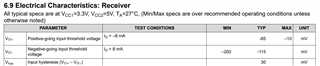
Hello, I would like to understand the input requirements of the ISO3088 A little better. Figure 6-10 shows minimum recommended Differential Input Voltage vs Signal Rate. I am running at 10Mbps so it recommends a differential voltage of about 650mV.
Say I have a square wave as the input signal. Does graph 6-10 mean the voltage from the top of my square wave to the base of my square wave should be 650mV total swing or does it require +650mV to -650mV. I have seen the definitions of Vid in Figure 7-7. There is no accompanying waveform so I am unclear.
If the input hysteresis thresholds are all between -200mV and -10mV (Table 6.9), why does Fig 6-10 recommend a 600mV swing all the way down to DC? The A/B input schematics in 8.4.1 don't look to me like a traditional differential amplifer (unless that emitter current source is shared between the inputs). Is it possible to share a more detailed schematic of the differential input section?
Hello Mark,
Good questions. The A and B pins only need to have a differential voltage that passes VIT+ or VIT- to change state. As you showed in table 6.9 this is -200mV to -10mV. The recommendation of VID > 600mV is to allow for headroom to improve signal integrity. Without this margin, small fluctuations in the differential signal could cause missed bits and data errors.
Unfortunately, I cannot share further details than what is shown in the device I/O schematics. However, please understand that this device is not a differential amplifier and the ISO3088 is a RS-485 transceiver and is intended to detect a differential digital signal.
For your reference, please see the ISO1410 which has clear waveform for typical operation of a RS-485 transceiver.
Best,
Andrew
So to frame it in my original terms, I should aim for a swing of +650mV to -650mV. Vid is an instantaneous measurement, not a waveform level measurement. For design purposes, the most relevant guideline is the recommended signal level figures and not the VTH+ / VTH- / VHYS spec.
www.ti.com/.../iso1410.pdf page 27
Equation 2: VID = VA – VB
--The receiver is enabled when the receiver enable pin, RE, is logic low.
--The receiver output, R, goes high when the differential input voltage defined by Equation 2 is greater than the positive input threshold, VTH+.
--The receiver output, R, goes low when the differential input voltage defined by Equation 2 is less than the negative input threshold, VTH–.
--If the VID voltage is between the VTH+ and VTH– thresholds, the output is indeterminate.
Yes. Everything here is correct.
I should aim for a swing of +650mV to -650mV.
Correct, +/-650mV is the recommended minimum differential swing for the receiver and signal integrity. As you have mentioned, are the VTH+ / VTH- / VHYS specs are design requirements that describe where the device will actually switch.
Best,
Andrew