This thread has been locked.

If you have a related question, please click the "Ask a related question" button in the top right corner. The newly created question will be automatically linked to this question.

SN6505B: Switching stops momentarity when ESD test

Part Number: SN6505B

Tool/software:

Hi team,

Our customer performed ESD test with this device, and observed switching stoped momentarity.

We guess this is because this device is disabled by EN pin or UVLO enable.

Please tell us about below question,

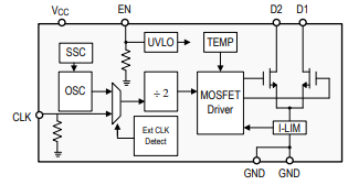
1. In datasheet 8.2 Block diagram, UVLO block is connected EN pin, but Table 5-1 says that UVLO is in Vcc description and the threshold is decides by Vcc voltage.
 Is this correct that UVLO is detected at Vcc pin?

2. How mach are there delay of device enable by EN pin and delay of UVLO enable after detected?

3. In this datasheet 8.4.5 External Clock Mode, it is said that "The device also has external clock fail safe feature which automatically switches the device to the internal clock if a valid input clock is not present for long (tCLKTIMER).". How does this device detect valid external clock?

4. EN pin and CLK pin is pulled-down by internal resister. How much is both of the resistance value?

5. In datasheet 8.2 Block diagram, there are two GND pin. Why is this?
  

Best regards,

teritama

  • Hi Teritama-san,

    Most team members are currently on time bank due to Christmas and New Year holidays. Please allow us to come back to you during the week of January 6, thanks.


    Regards,
    Koteshwar Rao

  • Hi Rao-san,

    Thank you for reply. Your teams help would be much appreciated.

    Do you have any update about this?

    Best regards,

    teritama

  • Hello Teritama-san, 

    Thank you for your patience. As you suggested the ESD could be toggling the EN pin and causing the device to shut down. One thought would be to tie the enable pin directly to VCC and apply ESD again to see if this improves the results.

    Please keep in mind that SN6505B is rated for ESD according to HBM and CDM standards. Both of these ESD models are for handling and manufacturing and do not require the device to have continuous operation while the ESD is applied. 

    1. In datasheet 8.2 Block diagram, UVLO block is connected EN pin, but Table 5-1 says that UVLO is in Vcc description and the threshold is decides by Vcc voltage.
       Is this correct that UVLO is detected at Vcc pin?
      1. Yes, UVLO is detected at the VCC pin and not the enable pin. However, the device will stop switching when enable pin is driven low. The block diagram shows that the UVLO block is used to shut down the device in both UVLO and EN low situations (8.4.3 Shutdown-Mode). 
    2. How mach are there delay of device enable by EN pin and delay of UVLO enable after detected?
      1. The device will power on according to the soft start feature to prevent inrush currents when the device is enabled by either the EN pin or when the VCC is above the UVLO+ threshold (8.4.1.1 Soft-Start).
    3. In this datasheet 8.4.5 External Clock Mode, it is said that "The device also has external clock fail safe feature which automatically switches the device to the internal clock if a valid input clock is not present for long (tCLKTIMER).". How does this device detect valid external clock?
      1. The device detects and clock input when the edges of a clock signal are present. The device will return to default switching when a clock edge has not been present after tCLKTIMER.
    4. EN pin and CLK pin is pulled-down by internal resister. How much is both of the resistance value?
      1. The value of the internal pull-down resistor on the EN and CLK pin of SN6505B-Q1 is ~500kΩ. 
    5. In datasheet 8.2 Block diagram, there are two GND pin. Why is this?
      1. The two ground pins are there to provide the IC a strong connection to the ground plane which will improve thermal performance. 

    Best,
    Andrew

  • Hello Andrew-san,

    Thank you for reply. I nunderstood your answer.

    About Q2 sorry for misunderstanding, I want to know about how time delay to shutdown after UVLO detected.

    Do you have any information about this?

    Best regards,

    teritama

  • In addition, about Q4, are there any requirement of edge of external clock signal?

  • Hello Teritama-san, 

    Thank you for the clarification. See the follow-up answers below.

    Q2 - I understand you are asking for the time it takes SN6505B to stop switching and discharge (shutdown) once the device is disabled at EN pin or UVLO is detected. Allow me some more time to look into this since it is not a datasheet spec. 

    Q4 - A valid clock input will follow the thresholds shown below. Please note that the spec is meant to be read proportional to Vcc. For example: (Vin(on) = VCC*0.7) is 3.5V when VCC=5V

    I hope this helps. 
    Best,
    Andrew

  • Hello,
    I got an answer back from the team quickly. 

    Q2 - As I said the earlier this is not a datasheet spec. Once UVLO is detected (or EN pin is disabled), the output will stop switching almost immediately. However, the output capacitors will require more time to discharge than any delay from the UVLO or shut down circuits. The time it takes SN6505 to stop switching is negligible compared to how long the output capacitors will take to discharge after switching has stopped.  

    Best,
    Andrew

  • Hello Andrew-san,

    Thank you for your answer.

    About Q2, how long the time to detect EN=Hi and UVLO? The customer want to know if it is possible or not that these function accure by momentary voltage fluctuations.

    And in the case of detected edge of one pulse, in my understanding, CLK mode is switch from internal mode to external mode.

    In the transition pireriod, does the switching of this device stop for minimum tCLKTIMER?

    Please comment your opinion.

    best regards,

    teritama

  • Hello Teritama-san, 

    The SN6505 can stop switching under the following conditions:

    • The EN pin will stop switching if the voltage on the pin is below VCC*0.3V. This is the spec VIN(OFF) - EN pin logic low threshold. 
    • The UVLO will stop device switching if the voltage on VCC is below the Negative-going UVLO threshold (VCC- (UVLO))

    The device may stop switching if a voltage causes either of the above conditions. 

    And in the case of detected edge of one pulse, in my understanding, CLK mode is switch from internal mode to external mode.

    In the transition pireriod, does the switching of this device stop for minimum tCLKTIMER?

    Yes, your understanding is correct. After a clock pulse is detected, the device waits for more edges in order to determine the frequency. Therefore, I would expect the transition period to be around the same as tCLKTIMER when switching from internal to external clocking. Unfortunately, this behavior is not currently listed as a datasheet speck. 

    Best,
    Andrew

  • Hello Andrew-san,

    I understand about device switching stop condition. Are there no requirement about detection time on EN and UVLO?

    For example. It require to stop switchin that Vcc is below the Negative-going UVLO threshold (VCC- (UVLO) for few nsec.

    Best regards,

    teritama

  • Hi Teritama-san,

    January 20th is holiday in the US. Please allow Andrew to review your question and get back to you later today, thanks.


    Regards,
    Koteshwar Rao

  • Hello Teritama-san, 

    There is not requirement for detection time. Once the VCC is below the (VCC- (UVLO)), the device UVLO will trigger and switching will stop. 

    Best,
    Andrew

  • Hi Andrew-san,

    Thank you for your kindly support. I understand.

    Best regards,

    teritama