


Part Number: ISO7762DWEVM
Tool/software:
Hello,
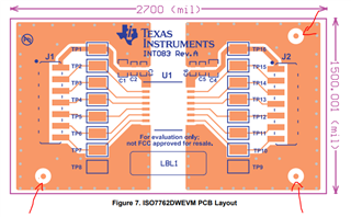
I have two questions relating to the ISO7762DWEVM. Is it a single layer PCB?
Also, what is the purpose of the three points shown below?
Part Number: ISO7762DWEVM
Tool/software:
Hello,
I have two questions relating to the ISO7762DWEVM. Is it a single layer PCB?
Also, what is the purpose of the three points shown below?
