This thread has been locked.

If you have a related question, please click the "Ask a related question" button in the top right corner. The newly created question will be automatically linked to this question.

ISOW1044: CREEPAGE AND CLEARANCE VS LAND PATTERN

Part Number: ISOW1044
Other Parts Discussed in Thread: ISOW7741,

Tool/software:

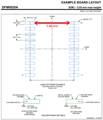
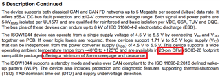
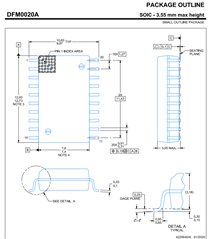
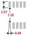
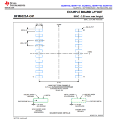
The component "ISOW1044DFMR" uses "DFM0020A" package, and according to the datasheet, this package provides a minimum creepage and clearance of 8 mm. However, when examining the land pattern dimensions, it appears that the clearance is actually below 8.00 mm, which is 7.60 mm. kindly assist us by providing a land pattern recommendation that includes defined creepage and clearance (Min. 8.00mm) and provide guidance on it. Attached snaps for your reference.

  • Hi Anand,

    Thank You for reaching. Please find my inputs below.

    1. First thing, you're referring to the land pattern to calculate package creepage/clearance which is not the right way.
    2. Land pattern shows exposed solder metal, which does not match with package(DFM0020A) dimensions. The exposed solder metal on PCB always has some extra metal compared to the contact region with the device pins.
    3. The device package itself has a minimum creepage/clearance on 8mm. Please refer package outline to understand the land pattern and device package pins do not overlap 100%

    Regards
    Varun
  • Hi Varun,

    Thanks for your prompt response,

    According to your response, I can understand the specified minimum creepage/clearance of 8.00 mm in the datasheet pertains to the package level and it is not intended for the land pattern.

    We utilize a unique land pattern calculator tool to determine the pad dimensions and spacing. Based on its output, the clearance between the adjacent pads was 7.30 mm (see attached snap), whereas the datasheet recommended a clearance of 7.60 mm.

    Could you kindly clarify if it is required to adhere to the datasheet's recommended spacing to maintain creepage and clearance for HV/Isolation, or can we use our calculated values instead?

    Out of curiosity, I noticed two distinct land pattern suggestions for certain parts, indicating that one follows the IPC7351 standard while the other features the HV/Isolation option. Do we possess similar patterns for our component?

  • Hi Anand,

    Thanks for further clarification. Apologies for the confusion before.

    If the ask is to have a land pattern which gives minimum clearance and creepage of 8mm then please refer to ISOW7741 datasheet land pattern(attaching the snap below).

    Both ISOW7741 and ISOW1044 are 20DFM package, so the land pattern of ISOW7741 can be used for ISOW1044 as well. This will give you your desired 8mm clearance/creepage solution.

    Regards
    Varun