


Other Parts Discussed in Thread: ISO6741
Tool/software:
Hi team,
We have a few questions about the PCB layout guidance of ISO6741:
1. Why is the layer spacing required to be this value? What is the impact on high-frequency signals? Will the same spacing be applicable to other TI isolation chips?
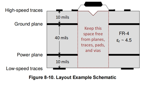
2. Is it allowed to drill holes and lay copper under the isolation chip? There is a sentence in the data sheet, but the reason is not explained in detail. Is it okay if only holes are drilled?
3. What level of EMC test has this ISO6741 chip passed? Can you show us the test report?
BR,
Ethan
