This thread has been locked.

If you have a related question, please click the "Ask a related question" button in the top right corner. The newly created question will be automatically linked to this question.

ISO6741-Q1: Power dissipation calculation verification

Part Number: ISO6741-Q1

Tool/software:

Dear TI team,

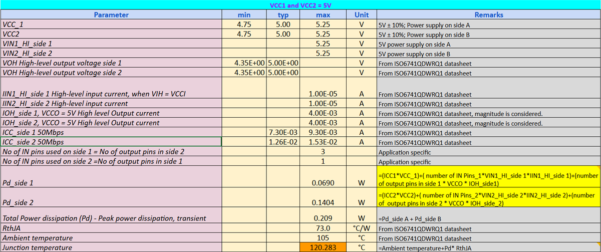
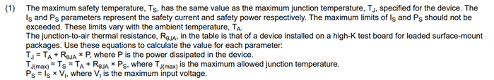
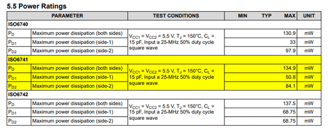
1) Please check the power dissipation calculation for ISO6741QDWRQ1 IC as shown below. The calculated value (209mW) exceeds the datasheet maximum power dissipation value_both sides (134.6mW). If the calculated value is wrong, please provide the right method for calculating the total power dissipation and the junction temperature. 

2) 

  • Hi Srijeeth,

    Thanks for reaching out.

    Please allow me to double check this. From a quick look, it seems that the test conditions of the power dissipation are different.

    (120.283-105)/73 = 209mW

    Can you please clarify why TA = 105C, Tj = 120.283? are these measured values from your system?

    This is an Additional resource that may be helpful for you: Semiconductor and IC Package Thermal Metrics (Rev. D)

    Regards,
    Aaditya V.

  • Hi Aaditya,

    Thank you for the response.

    By considering an ambient temperature as 105°C, the mathematical calculated junction temperature is obtained as 120.283°C. The calculation for the power dissipation is mentioned in the 'remarks' column. While we perform a hardware test to verify this, we also wanted to verify through calculations. 

  • Hi Srijeeth,

    So just to understand your calculations, please correct me if my understanding is incorrect:

    TA = 105C is a temperature that you have assigned to be your systems ambient temperature. Tj is the junction temperature calculated by you by using Ta and Pd. Pd is the power dissipation was calculated based on the Vcc and Icc of your system.

    Please see below how the power dissipation of 134mW is calculated in our datasheet:

    As you can see in the table, the VCC is 5.5V, which is max voltage of recommended operating conditions. The input signal is 25MHz (50Mbps) and Tj is 150C (from the absolute maximum ratings). if you look at the supply characteristics table, you can see that the ICC1 and ICC2 for 50Mbps (max) is 9.3mA and 15.3mA. This means that PD1 and PD2 would be 50.8mW and 84.1mW respectively. 

    Considering the above, the power dissipation values will be different if the Tj and the Ta are different compared to the test conditions in the table. Some clarity on the calculations would be helpful in relation to your system.

    Regards,
    Aaditya V

  • Hi Aaditya,

    May I know why is the power dissipation in individual input pins (INx) and output pins (OUTx) are not considered  ?

  • Hi Srijeeth,

    Power dissipation considers all the pins on each side of the isolator, not just the supply. From my previous post, you can see that the test conditions are at the max data rate, which would be the worst case power dissipation for that specific Ta and Tj.

    Additionally, the power dissipation is based on the current consumption ICC of each side, which can be found on the supply current characteristics. These specs consider all pins on each side separately.

    Regards,

    Aaditya