ISO1228EVM: Possible design by ISO1228 for health diagnostic

Part Number: ISO1228EVM
Other Parts Discussed in Thread: ISO1228, , ISO1228DFBEVM

Tool/software:

Hi,

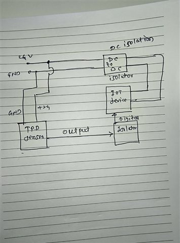
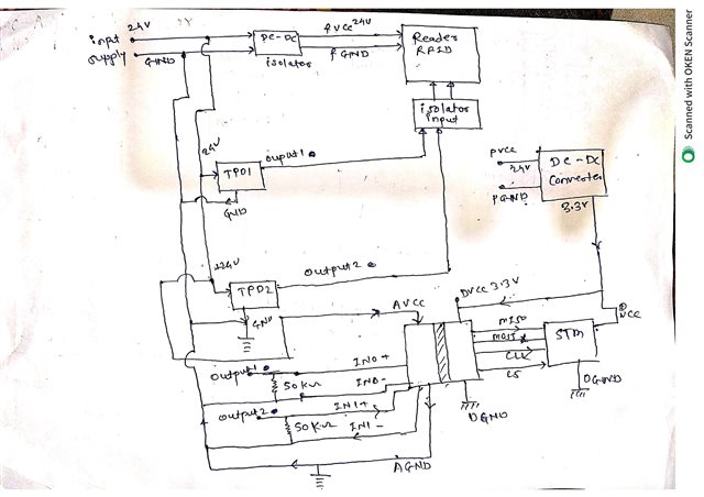
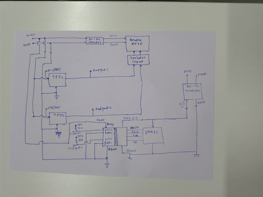
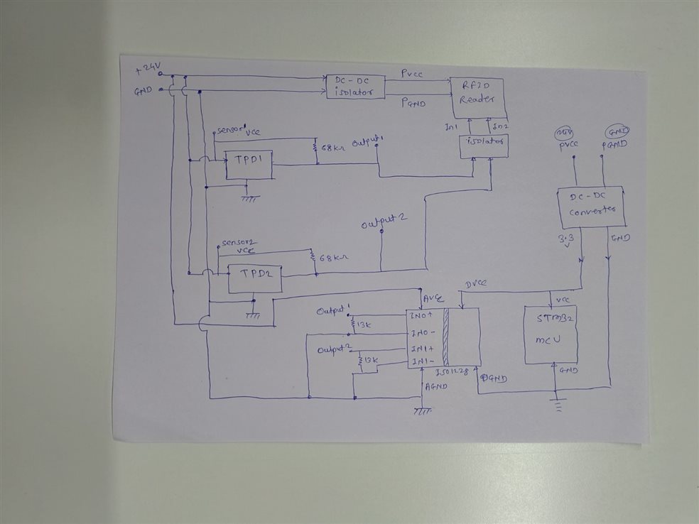
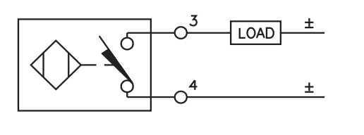
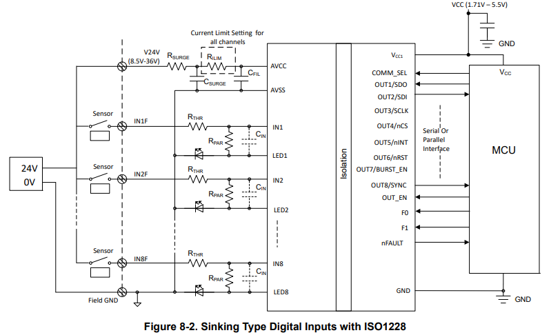
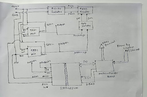
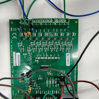
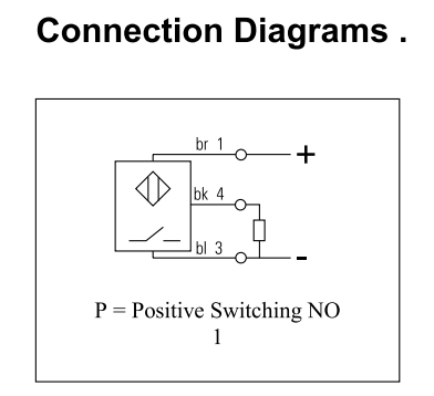
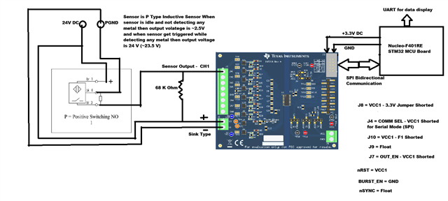
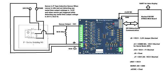
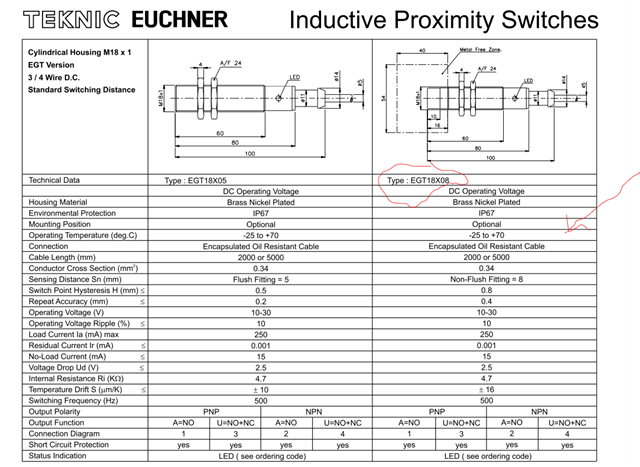
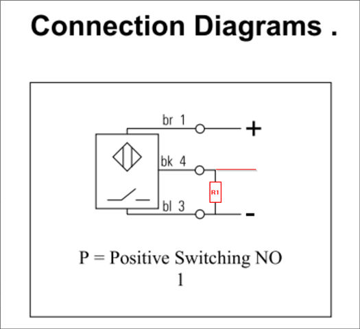
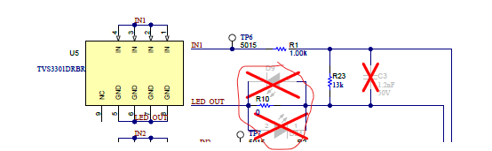
I have inductive TPD PNP sensor, Part No # NI75U-Q80-VP4X1-H1141 connected via Isolator IC as input to IoT device. See the block diagram.
I want to make another Embedded MCU based device to get health of TPD sensor and want to detect fault conditions.
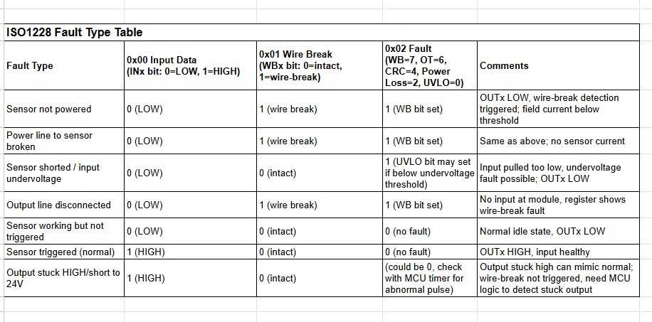
1) Sensor not powered ON
2) Sensor Short
3) Output line/wire break from isolator and floating
there are the three fault conditions for my logic.
So I want to connect one more mcu based device and want diagnose these details either by power path or output path.
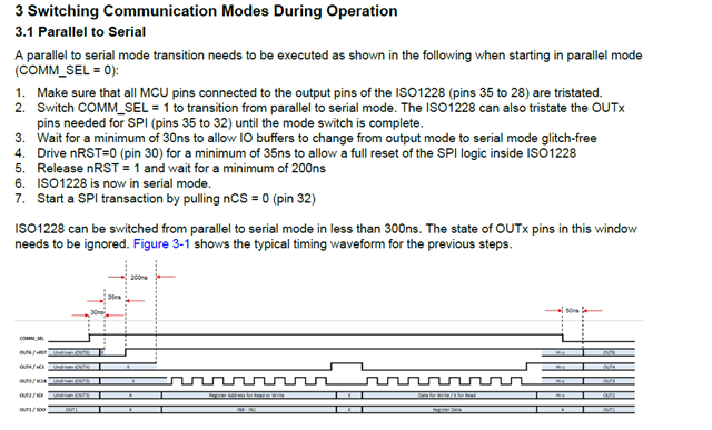
I thinking to use ISO1228 on output line which has output either parallel mode or serial mode which I can use to MCU for analysis. Is it possible
to detect these above mentioned conditions by using this ISO1228?

  • I want to meet these logic. Is it possible 

    Scenario/ Fault Type ISO1228 OUTx (GPIO Pin Input) SPI `IN_STAT` Bit SPI `DGN_STAT` Bit Comment
    Sensor not powered LOW 0 `OW_Dx = 1` Open-wire bit set, no input voltage, OUTx is LOW
    Power line to sensor broken LOW 0 `OW_Dx = 1` Same as above
    Sensor shorted LOW 0 `UV_Dx = 1` Input is pulled too low, undervoltage fault
    Output line disconnected LOW 0 `OW_Dx = 1` No voltage seen at input, OUTx remains LOW
    Sensor working but no trigger LOW 0 `OW_Dx = 0` No fault, just idle low — logic LOW
    Sensor triggered (normal) HIGH 1 `OW_Dx = 0`, `UV_Dx = 0` Everything healthy, sensor outputting 24V → OUT HIGH
  • Hello Sudeep, 

    Please allow me to Friday to review the information. 

  • Hello Andrew J,

    Sure, I am waiting for your forthcoming response. And Thanks for your valuable support. 

  • Hello Sudeep, 

    For the first 3 fault conditions: 

    1. Sensor not powered ON - The ISO1228 could detect of the field side AVCC/AVSS has lost power and will report it to the fault register. This may correspond to the sensor being powered off if they share the same power rail, but it will depend on system design. 
    2. Sensor Short - A short from the sensor will likely look the same as a valid logic input for the ISO1228. You could consider using another isolated device or channel of the ISO1228 to monitor if the sensor is stuck or shorted. 
    3. Output line/wire break from isolator and floating - This is supported. The ISO1228 has integrated wire-break detection and can detect if the connection to sensor is removed or broken. 

    The truth table above should be correct. Unless the sensor is shorted to VCC which will look like a valid logic signal to the ISO1228. The fault register can be monitored to detect which channel has a fault condition. 

    Best,
    Andrew

  • Hi Andrew, 

    Thank you so much for your valuable response. And great to hear positive response about my thinking vs response. It will very helpful to get about sensor health monitoring. I have got some other suggestions about connection, isolation etc as below, Please verify and confirm.  

    ISO1228 Wiring with PNP Sensor (NI75U-Q80-VP4X1-H1141) and STM32

    1. Field Side (Sensor Side – 24 V)

    Sensor Pin Connect To

    Brown +24 V DC

    Blue GND (same GND as ISO1228 AVSS)

    Black ISO1228 IN0+ (or any channel INx+)

    ISO1228 Field Side Pin Connect To Notes

    AVCC +24 V Same 24 V rail powering the sensor

    AVSS GND Common ground with sensor

    IN0+ (or INx+) Sensor Output Connect black wire of PNP sensor

    IN0– (or INx–) Leave floating or AVSS Optional for single-ended PNP input

    1. Logic Side (STM32 – 3.3 V or 5 V)

    ISO1228 Logic Side Pin Connect To Notes

    DVCC 3.3 V or 5 V Depends on STM32 logic level

    DGND GND Ground of STM32

    OUT0 (or OUTx) STM32 GPIO input Optional — logic level change detection (in parallel with SPI)

    nFAULT STM32 GPIO input Active-low fault indication

    SCLK STM32 SPI SCK

    SDI STM32 SPI MOSI

    SDO STM32 SPI MISO

    CS STM32 SPI NSS

    Wrench Note: Use a 100 Ω resistor in series on SPI lines if you're running at high clock speeds, as suggested in ISO1228EVM hardware.

    1. Grounding Notes

    AVSS (sensor-side GND) and DGND (STM32 side GND) are isolated internally in ISO1228.

    Do NOT connect them together.

    This is what gives galvanic isolation between sensor power and logic domain.

    1. Recommended Startup Configuration

    Configure ISO1228 in Parallel Mode for OUTx pins OR

    Use SPI Mode to read:

    IN_STAT register for logic level (HIGH/LOW)

    DGN_STAT register for:

    OW_Dx = Open wire

    UV_Dx = Undervoltage (e.g., short to GND)

    Fault Type ISO1228 OUTx (GPIO Pin Input) SPI `IN_STAT` Bit SPI `DGN_STAT` Bit Comment
    Sensor not powered LOW 0 OW_Dx = 1 Open-wire bit set, no input voltage, OUTx is LOW
    Power line to sensor broken LOW 0 OW_Dx = 1 Same as above
    Sensor shorted LOW 0 UV_Dx = 1 Input is pulled too low, undervoltage fault
    Output line disconnected LOW 0 OW_Dx = 1 No voltage seen at input, OUTx remains LOW
    Sensor working but no trigger LOW 0 OW_Dx = 0 No fault, just idle low — logic LOW
    Sensor triggered (normal) HIGH 1 OW_Dx = 0, UV_Dx = 0 Everything healthy, sensor outputting 24V → OUT HIGH
    Output stuck HIGH / short to 24 V HIGH 1 OW_Dx = 0, UV_Dx = 0 Warning Looks like normal HIGH — use MCU timer to detect


  • Hi Andrew, 
    Most of the above points look correct. One comment in your table below. 

    Fault Type ISO1228 OUTx (GPIO Pin Input) SPI `IN_STAT` Bit SPI `DGN_STAT` Bit Comment
    Sensor not powered LOW 0 OW_Dx = 1 Open-wire bit set, no input voltage, OUTx is LOW - This is partially true. A small resistance is needed accoss the sensor in order to have some current draw which the ISO1228 accepts as the sensor is connected. Please see 8.2.3.1.3 Wire-Break Detection for more details. 
    Power line to sensor broken LOW 0 OW_Dx = 1 Same as above
    Sensor shorted LOW 0 UV_Dx = 1 Input is pulled too low, undervoltage fault
    Output line disconnected LOW 0 OW_Dx = 1 No voltage seen at input, OUTx remains LOW
    Sensor working but no trigger LOW 0 OW_Dx = 0 No fault, just idle low — logic LOW
    Sensor triggered (normal) HIGH 1 OW_Dx = 0, UV_Dx = 0 Everything healthy, sensor outputting 24V → OUT HIGH
    Output stuck HIGH / short to 24 V HIGH 1 OW_Dx = 0, UV_Dx = 0 Warning Looks like normal HIGH — use MCU timer to detect

    The other comments seem to match datasheet recommendations and the configurations of both EVMs. Please let me know if you have further questions.

    Best,
    Andrew

  • Hello Andrew, 

    I think ISO1228EVK have already small resistance that you suggested for first point. Can you please confirm? So that Can I test my requirement with this EVM board otherwise I need to add small resistance externally. Can you suggest value of resistance? and also Can I refer the reference circuit given in ISO1228EVM manual. I am referring www.ti.com/.../ISO1228DFBEVM
    C
    an you guide about how to connect this small resistance. I mean between Output of sensor line and GND?

  • Hello Sudeep, 

    One quick clarification, when I said "small resistance" I mean a "small current" should be across the sensor in the OFF state to indicate that the sensor is still connected when OFF. This is typically around 50koms (24V/400uA = 60k). The small current needs to be above the 245uA threshold (wire break detection threshold) in order to trigger the fault.

    The resistance needs to be in parallel with the sensor. See the section on page 2 "Proposed solution for wire-break detection and diagnostics" (How to implement wire‐break detection and diagnostics in isolated digital inputs (Rev. A)). 

    Best,
    Andrew

  • Hello Andrew,

    Thank you once again for your guidance.

    I have reviewed all our previous conversations and the documents you suggested. Based on my understanding, I have drawn the final block diagram and shared it here for your confirmation. Please check and let me know if my understanding is correct.

    In this design, I am using two sensors, each with an output line (Output1 and Output2) connected to the RFID reader through an isolator. Additionally, Output1 is connected to IN0+ of the ISO1228, and Output2 is connected to IN1+ of the ISO1228. I am using two channels. A 50 kΩ resistor is placed across IN0+ and IN0-, and another 50 kΩ resistor is placed across IN1+ and IN1-.

    I have a couple of follow-up questions:

    1. Sensor not powered – As per my understanding, AVCC is directly connected to the sensor power supply, and sensor ground is connected to AGND. So, if the sensor is not powered or if its supply wire breaks, then the SPI IN_STAT bit should be 0 and OW_Dx = 1. Is this correct?

    2. Installation layout – All devices and the ISO1228 circuitry will be installed inside a railway location box near the control panel. I have attached images for reference. The PNP-type TPD sensor will be installed on the train track to detect wheel count. From the panel, only +24 V supply, GND, and the sensor’s output wire will run to the sensor; the output will return to the location box. In the block diagram, only the sensor is outside, and all other components are inside the location box near the control panel. Can you confirm if my understanding is correct, and whether this setup will allow detection of whether the sensor is powered or not?

  • Hello Sudeep, 

    The block diagram looks good. One comment: RPAR should either be 13k or 9.76k to set the current limit. 50kohms is to high for this. 

    As for the other questions see below:

    1. Sensor not powered – As per my understanding, AVCC is directly connected to the sensor power supply, and sensor ground is connected to AGND. So, if the sensor is not powered or if its supply wire breaks, then the SPI IN_STAT bit should be 0 and OW_Dx = 1. Is this correct?

      1. If the ISO1228 power connection is maintained and the sensor is not powered, then yes, the wire break but would be triggered.
      2. If the ISO1228 itself looses power, then the field power loss bit would be triggered and not wire break. 
      3. AVCC and the sensors can use the same power supply. AVCC can also be powered from an independent supply if needed. 
    2. Installation layout – All devices and the ISO1228 circuitry will be installed inside a railway location box near the control panel. I have attached images for reference. The PNP-type TPD sensor will be installed on the train track to detect wheel count. From the panel, only +24 V supply, GND, and the sensor’s output wire will run to the sensor; the output will return to the location box. In the block diagram, only the sensor is outside, and all other components are inside the location box near the control panel. Can you confirm if my understanding is correct, and whether this setup will allow detection of whether the sensor is powered or not?

      1. Yes, I believe your understanding is correct. Although the TPD sensors will need a small current ~400uA  draw when the switch is open to indicate that it is connected and powered (wire-break detection current in the datasheet). This can be done with a resistor from 24V to OUTPUT in parallel with each TPD sensor as discussed in the previous reply. 
  • Hi Andrew,

    I have shared here two block diagrams need your suggestion which one is correct understanding. 

    Block Diagram 1 : 

    So, based on your explanation, in the diagram I shared earlier, the 50 kΩ resistor should be replaced with either 13 kΩ or 9.76 kΩ. Also, it is not connected between IN0+ and IN0- (Output and AGND), but instead between IN0+ and the sensor power +24 V, correct? And IN0- should remain connected to AGND as it is. same for second sensor. 

    Block Diagram 2: 

    The 50 kΩ resistor should be replaced with either 13 kΩ or 9.76 kΩ.
    It should be connected between IN0+ and IN0− (Output and AGND).
    Additionally, a small resistor of approximately 68 kΩ should be connected between the 24 V supply and the sensor output.
    Apply the same configuration for the second sensor.

    One more point — if I connect this  resistor between the sensor power and IN0+ (sensor output), the isolator in the device will always see a HIGH state. Currently, it stays LOW when there is no event, and goes HIGH only when an event occurs. Is my understanding correct?

    If that’s the case, then I’ll need to update the RFID reader code logic, because at present the reader interprets LOW as the idle condition and HIGH as the event. Adding this resistor would reverse that logic.because we have no added any pullup register on input sense and sensor also PNP. 

    Please see both diagram and share which one understanding is correct. Also second question about logic state also important for my understanding so please guide. 
    Waiting for your forthcoming response. I have ordered the ISO1228EVK also for testing so before that I need to clear my doubts. 

  • Hello Sudeep, 

    From my understanding the second diagram is the correct setup of your system using ISO1228. From my understanding your sensor is similar to the following diagram (please share a more accurate picture if it is not correct):

    For this type of sensor the PNP inductive sensor will "switch" to a short when proximity is detected. The ISO1228 is designed to work with sensors like this and the connection is as simple as shown in the datasheet. 

    All that said, your second diagram looks good. 

    Best,
    Andrew

  • Hello Andrew, 

    Thanks for clarity. I am working on it. I will update you next 7-8 days about my work. 

  • Hello Andrew,

    Thank you for all your support. I have received the ISO1228EVM board and completed some basic testing following the connection details shown in the shared block diagram.

    In the block diagram, I am using a Nucleo-F401RE board connected via SPI to the ISO1228EVM. The secondary side 3.3V power supply for the ISO1228EVM is provided by the Nucleo-F401RE board, which itself is powered by the 5V USB supply from my laptop.

    I am reading SPI registers 00h, 01h, and 02h, and have built logic to extract all the status bits. The results are sent to a serial terminal via the UART of the STM32 board. The output I am getting is:

    Inputs: 00000000<LF>
    WireBrk: 00000000<LF>
    Faults: 00000000<LF>
    Ch1: OFF (Idle/Not triggered)<LF>
    <LF>
    Ch2: OFF (Idle/Not triggered)<LF>
    <LF>
    Ch3: OFF (Idle/Not triggered)<LF>
    <LF>
    Ch4: OFF (Idle/Not triggered)<LF>
    <LF>
    Ch5: OFF (Idle/Not triggered)<LF>
    <LF>
    Ch6: OFF (Idle/Not triggered)<LF>
    <LF>
    Ch7: OFF (Idle/Not triggered)<LF>
    <LF>
    Ch8: OFF (Idle/Not triggered)<LF>
    <LF>
    --- FAULT bits: WB:0 OT:0 CRC:0 PL:0 UVLO:0 ---<LF>

    On the input side, I am providing 24V as per the block diagram, with a 68kΩ resistor connected between the sensor outputs and the 24V supply, as shown.

    I have set the COM_SEL pin to VCC for serial communication mode, with F0/F1 pins both LOW/GND, and OUT_EN enabled (connected to VCC). However, no valid data is read via SPI in this setup.

    In another test, I used parallel mode by setting COM_SEL to GND. Here, I observed unusual behavior: when the sensor output is connected to CH1 of the ISO1228, I get 3.3V, and when disconnected, 0V. But when connected to CH2, the voltage reads approximately 0.833V, dropping to 0V when disconnected.

    I would like to understand this behavior better and would appreciate your guidance. I have shared the block diagram and my STM32 code for reference.

    Please advise if I am missing or doing anything wrong.


    /* USER CODE BEGIN Header */
    /**
      ******************************************************************************
      * @file           : main.c
      * @brief          : Main program body
      ******************************************************************************
      * @attention
      *
      * Copyright (c) 2025 STMicroelectronics.
      * All rights reserved.
      *
      * This software is licensed under terms that can be found in the LICENSE file
      * in the root directory of this software component.
      * If no LICENSE file comes with this software, it is provided AS-IS.
      *
      ******************************************************************************
      */
    /* USER CODE END Header */
    /* Includes ------------------------------------------------------------------*/
    #include "main.h"
    
    /* Private includes ----------------------------------------------------------*/
    /* USER CODE BEGIN Includes */
    #include <stdio.h>
    #include <string.h>
    /* USER CODE END Includes */
    
    /* Private typedef -----------------------------------------------------------*/
    /* USER CODE BEGIN PTD */
    
    /* USER CODE END PTD */
    
    /* Private define ------------------------------------------------------------*/
    /* USER CODE BEGIN PD */
    
    /* USER CODE END PD */
    
    /* Private macro -------------------------------------------------------------*/
    /* USER CODE BEGIN PM */
    #define ISO1228_SPI_CS_PORT   SP3I_CS_GPIO_Port
    #define ISO1228_SPI_CS_PIN    SP3I_CS_Pin
    
    /* USER CODE END PM */
    
    /* Private variables ---------------------------------------------------------*/
    SPI_HandleTypeDef hspi3;
    
    UART_HandleTypeDef huart2;
    
    /* USER CODE BEGIN PV */
    uint8_t iso_inputs;
    char uart_buf[32];
    char bin_str[9];
    
    char uart_buf1[32], uart_buf2[32], uart_buf3[32];
    
    uint8_t reg0_inputs, reg1_wb, reg2_fault;
    char bin_str0[9], bin_str1[9], bin_str2[9];
    
    /* USER CODE END PV */
    
    /* Private function prototypes -----------------------------------------------*/
    void SystemClock_Config(void);
    static void MX_GPIO_Init(void);
    static void MX_USART2_UART_Init(void);
    static void MX_SPI3_Init(void);
    /* USER CODE BEGIN PFP */
    
    /* USER CODE END PFP */
    
    /* Private user code ---------------------------------------------------------*/
    /* USER CODE BEGIN 0 */
    void ISO1228_Select(void) {
        HAL_GPIO_WritePin(ISO1228_SPI_CS_PORT, ISO1228_SPI_CS_PIN, GPIO_PIN_RESET); // CS LOW
    }
    
    void ISO1228_Deselect(void) {
        HAL_GPIO_WritePin(ISO1228_SPI_CS_PORT, ISO1228_SPI_CS_PIN, GPIO_PIN_SET);   // CS HIGH
    }
    
    // Reads register at `regAddr` from ISO1228
    HAL_StatusTypeDef ISO1228_ReadReg(uint8_t regAddr, uint8_t *regValue) {
        uint8_t txBuf[2], rxBuf[2];
        HAL_StatusTypeDef status;
    
        // Address phase: MSB=0 (read), lower 7 bits = address (0x00 for input reg)
        txBuf[0] = (0x00 << 7) | (regAddr & 0x7F); // 0x00 for Reg0
    
        // SPI transaction:
        ISO1228_Select();
        status = HAL_SPI_TransmitReceive(&hspi3, &txBuf[0], &rxBuf[0], 1, HAL_MAX_DELAY); // Send address
        if (status != HAL_OK) {
            ISO1228_Deselect();
            return status;
        }
        // Address phase done, now data phase: TX any (0x00), RX gets data
        txBuf[1] = 0x00;
        status = HAL_SPI_TransmitReceive(&hspi3, &txBuf[1], &rxBuf[1], 1, HAL_MAX_DELAY);
        ISO1228_Deselect();
    
        if (status == HAL_OK) *regValue = rxBuf[1];
        return status;
    }
    
    void print_sensor_status(uint8_t reg0_inputs, uint8_t reg1_wb, uint8_t reg2_fault)
    {
        char status_buf[100];
        int wb_fault   = (reg2_fault >> 7) & 1;   // Any wire-break present
        int ot_fault   = (reg2_fault >> 6) & 1;   // Over-temp
        int crc_fault  = (reg2_fault >> 4) & 1;   // CRC
        int pl_fault   = (reg2_fault >> 2) & 1;   // Power loss
        int uvlo_fault = (reg2_fault     ) & 1;   // UVLO
    
        for (int i = 0; i < 8; i++) {
            int input = (reg0_inputs >> i) & 1;
            int wb    = (reg1_wb    >> i) & 1;
            const char* status = "Unknown";
    
            if (wb)                 status = "FAULTY (Wire Break)\n";
            else if (wb_fault)      status = "FAULTY (Summary Wire Break)\n";
            else if (ot_fault)      status = "FAULTY (Over-temperature)\n";
            else if (crc_fault)     status = "FAULTY (CRC error)\n";
            else if (pl_fault)      status = "FAULTY (Field Power Loss)\n";
            else if (uvlo_fault)    status = "FAULTY (UVLO)\n";
            else if (input)         status = "ON (Triggered)\n";
            else                   status = "OFF (Idle/Not triggered)\n";
    
            snprintf(status_buf, sizeof(status_buf), "Ch%d: %s\n", i+1, status);
            HAL_UART_Transmit(&huart2, (uint8_t*)status_buf, strlen(status_buf), HAL_MAX_DELAY);
        }
        sprintf(status_buf, "--- FAULT bits: WB:%d OT:%d CRC:%d PL:%d UVLO:%d ---\n", wb_fault, ot_fault, crc_fault, pl_fault, uvlo_fault);
        HAL_UART_Transmit(&huart2, (uint8_t*)status_buf, strlen(status_buf), HAL_MAX_DELAY);
    }
    
    
    // Converts 8-bit value to binary text
    void bin8_to_str(uint8_t val, char* str) {
        for (int i = 7; i >= 0; --i)
            str[7-i] = (val & (1<<i)) ? '1' : '0';
        str[8] = '\0';
    }
    
    /* USER CODE END 0 */
    
    /**
      * @brief  The application entry point.
      * @retval int
      */
    int main(void)
    {
    
      /* USER CODE BEGIN 1 */
    
      /* USER CODE END 1 */
    
      /* MCU Configuration--------------------------------------------------------*/
    
      /* Reset of all peripherals, Initializes the Flash interface and the Systick. */
      HAL_Init();
    
      /* USER CODE BEGIN Init */
    
      /* USER CODE END Init */
    
      /* Configure the system clock */
      SystemClock_Config();
    
      /* USER CODE BEGIN SysInit */
    
      /* USER CODE END SysInit */
    
      /* Initialize all configured peripherals */
      MX_GPIO_Init();
      MX_USART2_UART_Init();
      MX_SPI3_Init();
      /* USER CODE BEGIN 2 */
     // HAL_UART_Transmit(&huart2, (uint8_t*)"Hello1\n", 7, HAL_MAX_DELAY);
    
      ISO1228_Deselect(); // Ensure CS is high
     // HAL_UART_Transmit(&huart2, (uint8_t*)"Hello2\n", 7, HAL_MAX_DELAY);
    
      /* USER CODE END 2 */
    
      /* Infinite loop */
      /* USER CODE BEGIN WHILE */
      while (1)
      {
        /* USER CODE END WHILE */
    
        /* USER CODE BEGIN 3 */
    	  // Read all three primary registers: Inputs, Wire-break, Fault
    	        HAL_StatusTypeDef s0, s1, s2;
    	        s0 = ISO1228_ReadReg(0x00, &reg0_inputs);
    	        s1 = ISO1228_ReadReg(0x01, &reg1_wb);
    	        s2 = ISO1228_ReadReg(0x02, &reg2_fault);
    
    	       // HAL_UART_Transmit(&huart2, (uint8_t*)"Hello3\n", 7, HAL_MAX_DELAY);
    
    	        if (s0 == HAL_OK && s1 == HAL_OK && s2 == HAL_OK)
    	        {
    	            bin8_to_str(reg0_inputs, bin_str0);
    	            bin8_to_str(reg1_wb, bin_str1);
    	            bin8_to_str(reg2_fault, bin_str2);
    
    	            //int len = snprintf(uart_buf, sizeof(uart_buf),"Inputs:   %s\r\nWireBrk:  %s\r\nFaults:   %s\r\n\r\n",bin_str0, bin_str1, bin_str2);
    	            //sprintf(uart_buf,"Inputs:   %s\r\nWireBrk:  %s\r\nFaults:   %s\r\n\r\n",bin_str0, bin_str1, bin_str2);
    	            memset((uint8_t *)uart_buf1, '\0', sizeof(uart_buf1));
    	            memset((uint8_t *)uart_buf2, '\0', sizeof(uart_buf2));
    	            memset((uint8_t *)uart_buf3, '\0', sizeof(uart_buf3));
    	            sprintf(uart_buf1,"Inputs:  %s\n", bin_str0);
    	            sprintf(uart_buf2,"WireBrk:  %s\n", bin_str1);
    	            sprintf(uart_buf3,"Faults:  %s\n", bin_str2);
    	            int len1 = strlen(uart_buf1);
    	            int len2 = strlen(uart_buf2);
    	            int len3 = strlen(uart_buf3);
    	           // HAL_UART_Transmit(&huart2, (uint8_t*)uart_buf, len, HAL_MAX_DELAY);
    	            HAL_UART_Transmit(&huart2, (uint8_t*)uart_buf1, len1, HAL_MAX_DELAY);
    	            HAL_UART_Transmit(&huart2, (uint8_t*)uart_buf2, len2, HAL_MAX_DELAY);
    	            HAL_UART_Transmit(&huart2, (uint8_t*)uart_buf3, len3, HAL_MAX_DELAY);
    	            print_sensor_status(reg0_inputs, reg1_wb, reg2_fault);
    
    	        }
    	        else
    	        {
    	            const char* err = "ISO1228 SPI read error\n";
    	            HAL_UART_Transmit(&huart2, (uint8_t*)err, strlen(err), HAL_MAX_DELAY);
    	        }
    	        HAL_Delay(500); // Adjust as needed
      }
      /* USER CODE END 3 */
    }
    
    /**
      * @brief System Clock Configuration
      * @retval None
      */
    void SystemClock_Config(void)
    {
      RCC_OscInitTypeDef RCC_OscInitStruct = {0};
      RCC_ClkInitTypeDef RCC_ClkInitStruct = {0};
    
      /** Configure the main internal regulator output voltage
      */
      __HAL_RCC_PWR_CLK_ENABLE();
      __HAL_PWR_VOLTAGESCALING_CONFIG(PWR_REGULATOR_VOLTAGE_SCALE2);
    
      /** Initializes the RCC Oscillators according to the specified parameters
      * in the RCC_OscInitTypeDef structure.
      */
      RCC_OscInitStruct.OscillatorType = RCC_OSCILLATORTYPE_HSI;
      RCC_OscInitStruct.HSIState = RCC_HSI_ON;
      RCC_OscInitStruct.HSICalibrationValue = RCC_HSICALIBRATION_DEFAULT;
      RCC_OscInitStruct.PLL.PLLState = RCC_PLL_ON;
      RCC_OscInitStruct.PLL.PLLSource = RCC_PLLSOURCE_HSI;
      RCC_OscInitStruct.PLL.PLLM = 16;
      RCC_OscInitStruct.PLL.PLLN = 336;
      RCC_OscInitStruct.PLL.PLLP = RCC_PLLP_DIV4;
      RCC_OscInitStruct.PLL.PLLQ = 7;
      if (HAL_RCC_OscConfig(&RCC_OscInitStruct) != HAL_OK)
      {
        Error_Handler();
      }
    
      /** Initializes the CPU, AHB and APB buses clocks
      */
      RCC_ClkInitStruct.ClockType = RCC_CLOCKTYPE_HCLK|RCC_CLOCKTYPE_SYSCLK
                                  |RCC_CLOCKTYPE_PCLK1|RCC_CLOCKTYPE_PCLK2;
      RCC_ClkInitStruct.SYSCLKSource = RCC_SYSCLKSOURCE_PLLCLK;
      RCC_ClkInitStruct.AHBCLKDivider = RCC_SYSCLK_DIV1;
      RCC_ClkInitStruct.APB1CLKDivider = RCC_HCLK_DIV2;
      RCC_ClkInitStruct.APB2CLKDivider = RCC_HCLK_DIV1;
    
      if (HAL_RCC_ClockConfig(&RCC_ClkInitStruct, FLASH_LATENCY_2) != HAL_OK)
      {
        Error_Handler();
      }
    }
    
    /**
      * @brief SPI3 Initialization Function
      * @param None
      * @retval None
      */
    static void MX_SPI3_Init(void)
    {
    
      /* USER CODE BEGIN SPI3_Init 0 */
    
      /* USER CODE END SPI3_Init 0 */
    
      /* USER CODE BEGIN SPI3_Init 1 */
    
      /* USER CODE END SPI3_Init 1 */
      /* SPI3 parameter configuration*/
      hspi3.Instance = SPI3;
      hspi3.Init.Mode = SPI_MODE_MASTER;
      hspi3.Init.Direction = SPI_DIRECTION_2LINES;
      hspi3.Init.DataSize = SPI_DATASIZE_8BIT;
      hspi3.Init.CLKPolarity = SPI_POLARITY_LOW;
      hspi3.Init.CLKPhase = SPI_PHASE_1EDGE;
      hspi3.Init.NSS = SPI_NSS_SOFT;
      hspi3.Init.BaudRatePrescaler = SPI_BAUDRATEPRESCALER_2;
      hspi3.Init.FirstBit = SPI_FIRSTBIT_MSB;
      hspi3.Init.TIMode = SPI_TIMODE_DISABLE;
      hspi3.Init.CRCCalculation = SPI_CRCCALCULATION_DISABLE;
      hspi3.Init.CRCPolynomial = 10;
      if (HAL_SPI_Init(&hspi3) != HAL_OK)
      {
        Error_Handler();
      }
      /* USER CODE BEGIN SPI3_Init 2 */
    
      /* USER CODE END SPI3_Init 2 */
    
    }
    
    /**
      * @brief USART2 Initialization Function
      * @param None
      * @retval None
      */
    static void MX_USART2_UART_Init(void)
    {
    
      /* USER CODE BEGIN USART2_Init 0 */
    
      /* USER CODE END USART2_Init 0 */
    
      /* USER CODE BEGIN USART2_Init 1 */
    
      /* USER CODE END USART2_Init 1 */
      huart2.Instance = USART2;
      huart2.Init.BaudRate = 115200;
      huart2.Init.WordLength = UART_WORDLENGTH_8B;
      huart2.Init.StopBits = UART_STOPBITS_1;
      huart2.Init.Parity = UART_PARITY_NONE;
      huart2.Init.Mode = UART_MODE_TX_RX;
      huart2.Init.HwFlowCtl = UART_HWCONTROL_NONE;
      huart2.Init.OverSampling = UART_OVERSAMPLING_16;
      if (HAL_UART_Init(&huart2) != HAL_OK)
      {
        Error_Handler();
      }
      /* USER CODE BEGIN USART2_Init 2 */
    
      /* USER CODE END USART2_Init 2 */
    
    }
    
    /**
      * @brief GPIO Initialization Function
      * @param None
      * @retval None
      */
    static void MX_GPIO_Init(void)
    {
      GPIO_InitTypeDef GPIO_InitStruct = {0};
    /* USER CODE BEGIN MX_GPIO_Init_1 */
    /* USER CODE END MX_GPIO_Init_1 */
    
      /* GPIO Ports Clock Enable */
      __HAL_RCC_GPIOC_CLK_ENABLE();
      __HAL_RCC_GPIOH_CLK_ENABLE();
      __HAL_RCC_GPIOA_CLK_ENABLE();
      __HAL_RCC_GPIOD_CLK_ENABLE();
      __HAL_RCC_GPIOB_CLK_ENABLE();
    
      /*Configure GPIO pin Output Level */
      HAL_GPIO_WritePin(LD2_GPIO_Port, LD2_Pin, GPIO_PIN_RESET);
    
      /*Configure GPIO pin Output Level */
      HAL_GPIO_WritePin(SP3I_CS_GPIO_Port, SP3I_CS_Pin, GPIO_PIN_RESET);
    
      /*Configure GPIO pin : B1_Pin */
      GPIO_InitStruct.Pin = B1_Pin;
      GPIO_InitStruct.Mode = GPIO_MODE_IT_FALLING;
      GPIO_InitStruct.Pull = GPIO_NOPULL;
      HAL_GPIO_Init(B1_GPIO_Port, &GPIO_InitStruct);
    
      /*Configure GPIO pin : LD2_Pin */
      GPIO_InitStruct.Pin = LD2_Pin;
      GPIO_InitStruct.Mode = GPIO_MODE_OUTPUT_PP;
      GPIO_InitStruct.Pull = GPIO_NOPULL;
      GPIO_InitStruct.Speed = GPIO_SPEED_FREQ_LOW;
      HAL_GPIO_Init(LD2_GPIO_Port, &GPIO_InitStruct);
    
      /*Configure GPIO pin : SP3I_CS_Pin */
      GPIO_InitStruct.Pin = SP3I_CS_Pin;
      GPIO_InitStruct.Mode = GPIO_MODE_OUTPUT_PP;
      GPIO_InitStruct.Pull = GPIO_NOPULL;
      GPIO_InitStruct.Speed = GPIO_SPEED_FREQ_LOW;
      HAL_GPIO_Init(SP3I_CS_GPIO_Port, &GPIO_InitStruct);
    
    /* USER CODE BEGIN MX_GPIO_Init_2 */
    /* USER CODE END MX_GPIO_Init_2 */
    }
    
    /* USER CODE BEGIN 4 */
    
    /* USER CODE END 4 */
    
    /**
      * @brief  This function is executed in case of error occurrence.
      * @retval None
      */
    void Error_Handler(void)
    {
      /* USER CODE BEGIN Error_Handler_Debug */
      /* User can add his own implementation to report the HAL error return state */
      __disable_irq();
      while (1)
      {
      }
      /* USER CODE END Error_Handler_Debug */
    }
    
    #ifdef  USE_FULL_ASSERT
    /**
      * @brief  Reports the name of the source file and the source line number
      *         where the assert_param error has occurred.
      * @param  file: pointer to the source file name
      * @param  line: assert_param error line source number
      * @retval None
      */
    void assert_failed(uint8_t *file, uint32_t line)
    {
      /* USER CODE BEGIN 6 */
      /* User can add his own implementation to report the file name and line number,
         ex: printf("Wrong parameters value: file %s on line %d\r\n", file, line) */
      /* USER CODE END 6 */
    }
    #endif /* USE_FULL_ASSERT */


  • Hello Sudeep, 

    Thank you for coming back! Since we are moving into more of a debug related discussion; I would like to confirm the operation of the EVM without going too far into the coding. 

    Before we start, please note the following:

    1. There are two EVMs for this device (the ISO1228EVM and the ISO1228DFBEVM).
      1. Assuming you have the ISO1228EVM, the board can be configured in either sink or source mode based on the connection of V1 (blue test point) and V2 (orange test point). 
    2. LEDx pins are tied together and connected to V1. 
    3. A rectifier bridge will ensure AVCC = 24V and AVSS = 0V when V1 and V2 are connected. 
      1. The device is in SINK mode when V1 = 0V and V2 = 24V
      2. The device is in SOURCE mode when V1 = 24V and V2 = 0V

    Now the simplest way to confirm the operation of ISO1228 EVM: 

    1. Disconnect the sensors and test the EVM by itself in parallel mode
    2. A single channel can be tested easily by connecting IN1 to either 24V or GND and observing OUTx (in parallel mode). 
      1. In SINK mode a short from INx to 24V will result in a OUT1 = 3.3V or 'HIGH'
      2. In SOURCE mode a short from INx to 0V will result in a OUT1 = 3.3V or 'HIGH
    3. Connect the MCU and test the device in serial mode. Repeat the same process by shorting IN1 and confirm the registers are reading a high at IN1. 

    Best,
    Andrew

  • Hello Andrew, 

    As you suggested I have checked EVM by itself in parallel mode. I am using ISO1228EVM.

    1) In SINK mode a short from INx to 24V will result in a OUT1 = 3.3V or 'HIGH'
    2) In SOURCE mode a short from INx to 0V will result in a OUT1 = 3.3V or 'HIGH'

    Both tests are working as you mentioned above.

    In Serial Mode , I have kept settings as below,
    COM_SEL = connected VCC = Serial Mode
    F0 = Left open = Float
    F1= connected to VCC
    nRST (OUT6) = High = Connected to VCC.
    BRST_EN (OUT7) = GND
    OUT_EN = VCC

    I have done connection in Sink mode.
    LEDx pins are tied together in my EVM but not showing any connectivity between V1 and LEDx pins.

    I am getting result now as below

    Inputs (0x00): 00000000<LF>
    WireBrk (0x01: 00000001<LF>
    Faults (0x02): 00000010<LF>
    Filter (0x03): 00000011<LF>
    Ch1: FAULTY (Wire Break)<CR><LF>
    Ch2: OFF (Idle/Not triggered)<CR><LF>
    Ch3: OFF (Idle/Not triggered)<CR><LF>
    Ch4: OFF (Idle/Not triggered)<CR><LF>
    Ch5: OFF (Idle/Not triggered)<CR><LF>
    Ch6: OFF (Idle/Not triggered)<CR><LF>
    Ch7: OFF (Idle/Not triggered)<CR><LF>
    Ch8: OFF (Idle/Not triggered)<CR><LF>
    Faults raw: 0x02 [WB:0 OT:0 CRC:0 PL:0 UVLO:0] UnknownMask:0x02<CR><LF>


    Here strange result Ch1 shows faulty in both condition
    a) When Ch1-Ch8 connected to 24V
    b) When Ch1-ch8 connected to 0V

    Same result as above if I connected either 24V to any input channel or 0V to any output channel.

    Can you look into it and guide further to get proper result.


    /* USER CODE BEGIN Header */
    /**
      ******************************************************************************
      * @file           : main.c
      * @brief          : Main program body
      ******************************************************************************
      * @attention
      *
      * Copyright (c) 2025 STMicroelectronics.
      * All rights reserved.
      *
      * This software is licensed under terms that can be found in the LICENSE file
      * in the root directory of this software component.
      * If no LICENSE file comes with this software, it is provided AS-IS.
      *
      ******************************************************************************
      */
    /* USER CODE END Header */
    /* Includes ------------------------------------------------------------------*/
    #include "main.h"
    
    /* Private includes ----------------------------------------------------------*/
    /* USER CODE BEGIN Includes */
    #include <stdio.h>
    #include <string.h>
    /* USER CODE END Includes */
    
    /* Private typedef -----------------------------------------------------------*/
    /* USER CODE BEGIN PTD */
    
    /* USER CODE END PTD */
    
    /* Private define ------------------------------------------------------------*/
    /* USER CODE BEGIN PD */
    
    /* USER CODE END PD */
    
    /* Private macro -------------------------------------------------------------*/
    /* USER CODE BEGIN PM */
    #define ISO1228_SPI_CS_PORT   SP3I_CS_GPIO_Port
    #define ISO1228_SPI_CS_PIN    SP3I_CS_Pin
    
    /* USER CODE END PM */
    
    /* Private variables ---------------------------------------------------------*/
    SPI_HandleTypeDef hspi3;
    
    UART_HandleTypeDef huart2;
    
    /* USER CODE BEGIN PV */
    uint8_t iso_inputs;
    char uart_buf[32];
    char bin_str[9];
    
    char uart_buf1[32], uart_buf2[32], uart_buf3[32], uart_buf4[32];
    
    uint8_t reg0_inputs, reg1_wb, reg2_fault, filter;
    char bin_str0[9], bin_str1[9], bin_str2[9], bin_str3[9];
    
    /* USER CODE END PV */
    
    /* Private function prototypes -----------------------------------------------*/
    void SystemClock_Config(void);
    static void MX_GPIO_Init(void);
    static void MX_USART2_UART_Init(void);
    
    static void MX_SPI3_Init(void);
    /* USER CODE BEGIN PFP */
    
    /* USER CODE END PFP */
    
    /* Private user code ---------------------------------------------------------*/
    /* USER CODE BEGIN 0 */
    void ISO1228_Select(void) {
        HAL_GPIO_WritePin(ISO1228_SPI_CS_PORT, ISO1228_SPI_CS_PIN, GPIO_PIN_RESET); // CS LOW
    }
    
    void ISO1228_Deselect(void) {
        HAL_GPIO_WritePin(ISO1228_SPI_CS_PORT, ISO1228_SPI_CS_PIN, GPIO_PIN_SET);   // CS HIGH
    }
    
    // Reads register at `regAddr` from ISO1228
    HAL_StatusTypeDef ISO1228_ReadReg(uint8_t regAddr, uint8_t *regValue) {
        uint8_t txBuf[2], rxBuf[2];
        HAL_StatusTypeDef status;
    
        // Address phase: MSB=0 (read), lower 7 bits = address (0x00 for input reg)
        txBuf[0] = (0x00 << 7) | (regAddr & 0x7F); // 0x00 for Reg0
    
        // SPI transaction:
        ISO1228_Select();
        status = HAL_SPI_TransmitReceive(&hspi3, &txBuf[0], &rxBuf[0], 1, HAL_MAX_DELAY); // Send address
        if (status != HAL_OK) {
            ISO1228_Deselect();
            return status;
        }
        // Address phase done, now data phase: TX any (0x00), RX gets data
        txBuf[1] = 0x00;
        status = HAL_SPI_TransmitReceive(&hspi3, &txBuf[1], &rxBuf[1], 1, HAL_MAX_DELAY);
        ISO1228_Deselect();
    
        if (status == HAL_OK) *regValue = rxBuf[1];
        return status;
    }
    
    static void print_faults(uint8_t f, UART_HandleTypeDef *uart)
    {
        char buf[128];
        int wb_sum = (f >> 7) & 1;   // Any channel WB
        int ot     = (f >> 6) & 1;   // Over-temp
        int crc    = (f >> 4) & 1;   // Inter-die CRC
        int pl     = (f >> 2) & 1;   // Field-side power loss
        int uvlo   = (f >> 0) & 1;   // MCU-side UVLO
        // Bits we didn’t explicitly decode (reserved)
        int unknown = f & ~((1<<7)|(1<<6)|(1<<4)|(1<<2)|(1<<0));
    
        int n = snprintf(buf, sizeof(buf),
            "Faults raw: 0x%02X  [WB:%d OT:%d CRC:%d PL:%d UVLO:%d] UnknownMask:0x%02X\r\n\n\n",
            f, wb_sum, ot, crc, pl, uvlo, unknown);
        HAL_UART_Transmit(uart, (uint8_t*)buf, n, HAL_MAX_DELAY);
    }
    
    void print_sensor_status(uint8_t reg0_inputs, uint8_t reg1_wb, uint8_t reg2_fault)
    {
        char status_buf[96];
        int wb_sum = (reg2_fault >> 7) & 1;
        int ot     = (reg2_fault >> 6) & 1;
        int crc    = (reg2_fault >> 4) & 1;
        int pl     = (reg2_fault >> 2) & 1;
        int uvlo   = (reg2_fault >> 0) & 1;
    
        // Per-channel, Ch1..Ch8 map to bit0..bit7
        for (int ch = 1; ch <= 8; ch++) {
            int bit = ch - 1;
            int input = (reg0_inputs >> bit) & 1;
            int wb    = (reg1_wb    >> bit) & 1;
    
            const char *status;
            if (wb)              status = "FAULTY (Wire Break)";
            else if (wb_sum)     status = "FAULTY (Summary Wire Break)";
            else if (ot)         status = "FAULTY (Over-temperature)";
            else if (crc)        status = "FAULTY (CRC error)";
            else if (pl)         status = "FAULTY (Field Power Loss)";
            else if (uvlo)       status = "FAULTY (UVLO)";
            else if (input)      status = "ON (Triggered)";
            else                 status = "OFF (Idle/Not triggered)";
    
            int n = snprintf(status_buf, sizeof(status_buf),
                             "Ch%d: %s\r\n", ch, status);
            HAL_UART_Transmit(&huart2, (uint8_t*)status_buf, n, HAL_MAX_DELAY);
        }
    
        // Summary line (decoded bits only) + show any unknown bits separately
        print_faults(reg2_fault, &huart2);
    }


    // Converts 8-bit value to binary text
    void bin8_to_str(uint8_t val, char* str) {
        for (int i = 7; i >= 0; --i)
            str[7-i] = (val & (1<<i)) ? '1' : '0';
        str[8] = '\0';
    }
    
    /* USER CODE END 0 */
    
    /**
      * @brief  The application entry point.
      * @retval int
      */
    int main(void)
    {
    
      /* USER CODE BEGIN 1 */
    
      /* USER CODE END 1 */
    
      /* MCU Configuration--------------------------------------------------------*/
    
      /* Reset of all peripherals, Initializes the Flash interface and the Systick. */
      HAL_Init();
    
      /* USER CODE BEGIN Init */
    
      /* USER CODE END Init */
    
      /* Configure the system clock */
      SystemClock_Config();
    
      /* USER CODE BEGIN SysInit */
    
      /* USER CODE END SysInit */
    
      /* Initialize all configured peripherals */
      MX_GPIO_Init();
      MX_USART2_UART_Init();
      MX_SPI3_Init();
      /* USER CODE BEGIN 2 */
     // HAL_UART_Transmit(&huart2, (uint8_t*)"Hello1\n", 7, HAL_MAX_DELAY);
    
      ISO1228_Deselect(); // Ensure CS is high
      HAL_Delay(30);  // >=25 ms after power-up per datasheet
    
    /*  {
          uint8_t tx[2] = {0x00, 0x00}, rx[2] = {0, 0};
          ISO1228_Select();
          HAL_SPI_TransmitReceive(&hspi3, &tx[0], &rx[0], 1, HAL_MAX_DELAY); // "address" phase (MOSI=0)
          HAL_SPI_TransmitReceive(&hspi3, &tx[1], &rx[1], 1, HAL_MAX_DELAY); // "data" phase (MOSI=0)
          ISO1228_Deselect();
    
          // rx[0] = O8..O1 (inputs) latched during address phase
          // rx[1] = Reg0 (inputs) latched during data phase
          char dbg[64];
          snprintf(dbg, sizeof(dbg), "SMOKE: rx0/O8..O1=0x%02X  rx1/Reg0=0x%02X\r\n", rx[0], rx[1]);
          HAL_UART_Transmit(&huart2, (uint8_t*)dbg, strlen(dbg), HAL_MAX_DELAY);
      }*/
    
    
     // HAL_UART_Transmit(&huart2, (uint8_t*)"Hello2\n", 7, HAL_MAX_DELAY);
    
      /* USER CODE END 2 */
    
      /* Infinite loop */
      /* USER CODE BEGIN WHILE */
      while (1)
      {
        /* USER CODE END WHILE */
    
        /* USER CODE BEGIN 3 */
    	  // Read all three primary registers: Inputs, Wire-break, Fault
    	        HAL_StatusTypeDef s0, s1, s2, s3;
    	        s0 = ISO1228_ReadReg(0x00, &reg0_inputs);
    	        s1 = ISO1228_ReadReg(0x01, &reg1_wb);
    	        s2 = ISO1228_ReadReg(0x02, &reg2_fault);
    	        s3 = ISO1228_ReadReg(0x03, &filter);
    
    
    	        if (s0 == HAL_OK && s1 == HAL_OK && s2 == HAL_OK && s3 == HAL_OK)
    	        {
    	            bin8_to_str(reg0_inputs, bin_str0);
    	            bin8_to_str(reg1_wb, bin_str1);
    	            bin8_to_str(reg2_fault, bin_str2);
    	            bin8_to_str(filter, bin_str3);
    
    	            memset((uint8_t *)uart_buf1, '\0', sizeof(uart_buf1));
    	            memset((uint8_t *)uart_buf2, '\0', sizeof(uart_buf2));
    	            memset((uint8_t *)uart_buf3, '\0', sizeof(uart_buf3));
    	            memset((uint8_t *)uart_buf4, '\0', sizeof(uart_buf4));
    	            sprintf(uart_buf1,"Inputs:  %s\n", bin_str0);
    	            sprintf(uart_buf2,"WireBrk:  %s\n", bin_str1);
    	            sprintf(uart_buf3,"Faults:  %s\n", bin_str2);
    	            sprintf(uart_buf4,"Filter:  %s\n", bin_str3);
    	            int len1 = strlen(uart_buf1);
    	            int len2 = strlen(uart_buf2);
    	            int len3 = strlen(uart_buf3);
    	            int len4 = strlen(uart_buf4);
    
    	            HAL_UART_Transmit(&huart2, (uint8_t*)uart_buf1, len1, HAL_MAX_DELAY);
    	            HAL_UART_Transmit(&huart2, (uint8_t*)uart_buf2, len2, HAL_MAX_DELAY);
    	            HAL_UART_Transmit(&huart2, (uint8_t*)uart_buf3, len3, HAL_MAX_DELAY);
    	            HAL_UART_Transmit(&huart2, (uint8_t*)uart_buf4, len4, HAL_MAX_DELAY);
    	            print_sensor_status(reg0_inputs, reg1_wb, reg2_fault);
    
    
    	        }
    	        else
    	        {
    	            const char* err = "ISO1228 SPI read error\n";
    	            HAL_UART_Transmit(&huart2, (uint8_t*)err, strlen(err), HAL_MAX_DELAY);
    	        }
    	            HAL_Delay(500); // Adjust as needed
      }
      /* USER CODE END 3 */
    }
    
    /**
      * @brief System Clock Configuration
      * @retval None
      */
    void SystemClock_Config(void)
    {
      RCC_OscInitTypeDef RCC_OscInitStruct = {0};
      RCC_ClkInitTypeDef RCC_ClkInitStruct = {0};
    
      /** Configure the main internal regulator output voltage
      */
      __HAL_RCC_PWR_CLK_ENABLE();
      __HAL_PWR_VOLTAGESCALING_CONFIG(PWR_REGULATOR_VOLTAGE_SCALE2);
    
      /** Initializes the RCC Oscillators according to the specified parameters
      * in the RCC_OscInitTypeDef structure.
      */
      RCC_OscInitStruct.OscillatorType = RCC_OSCILLATORTYPE_HSI;
      RCC_OscInitStruct.HSIState = RCC_HSI_ON;
      RCC_OscInitStruct.HSICalibrationValue = RCC_HSICALIBRATION_DEFAULT;
      RCC_OscInitStruct.PLL.PLLState = RCC_PLL_ON;
      RCC_OscInitStruct.PLL.PLLSource = RCC_PLLSOURCE_HSI;
      RCC_OscInitStruct.PLL.PLLM = 16;
      RCC_OscInitStruct.PLL.PLLN = 336;
      RCC_OscInitStruct.PLL.PLLP = RCC_PLLP_DIV4;
      RCC_OscInitStruct.PLL.PLLQ = 7;
      if (HAL_RCC_OscConfig(&RCC_OscInitStruct) != HAL_OK)
      {
        Error_Handler();
      }
    
      /** Initializes the CPU, AHB and APB buses clocks
      */
      RCC_ClkInitStruct.ClockType = RCC_CLOCKTYPE_HCLK|RCC_CLOCKTYPE_SYSCLK
                                  |RCC_CLOCKTYPE_PCLK1|RCC_CLOCKTYPE_PCLK2;
      RCC_ClkInitStruct.SYSCLKSource = RCC_SYSCLKSOURCE_PLLCLK;
      RCC_ClkInitStruct.AHBCLKDivider = RCC_SYSCLK_DIV1;
      RCC_ClkInitStruct.APB1CLKDivider = RCC_HCLK_DIV2;
      RCC_ClkInitStruct.APB2CLKDivider = RCC_HCLK_DIV1;
    
      if (HAL_RCC_ClockConfig(&RCC_ClkInitStruct, FLASH_LATENCY_2) != HAL_OK)
      {
        Error_Handler();
      }
    }
    
    /**
      * @brief SPI3 Initialization Function
      * @param None
      * @retval None
      */
    static void MX_SPI3_Init(void)
    {
    
      /* USER CODE BEGIN SPI3_Init 0 */
    
      /* USER CODE END SPI3_Init 0 */
    
      /* USER CODE BEGIN SPI3_Init 1 */
    
      /* USER CODE END SPI3_Init 1 */
      /* SPI3 parameter configuration*/
      hspi3.Instance = SPI3;
      hspi3.Init.Mode = SPI_MODE_MASTER;
      hspi3.Init.Direction = SPI_DIRECTION_2LINES;
      hspi3.Init.DataSize = SPI_DATASIZE_8BIT;
      hspi3.Init.CLKPolarity = SPI_POLARITY_LOW;
      hspi3.Init.CLKPhase = SPI_PHASE_1EDGE;
      hspi3.Init.NSS = SPI_NSS_SOFT;
      hspi3.Init.BaudRatePrescaler = SPI_BAUDRATEPRESCALER_128; //SPI_BAUDRATEPRESCALER_2;
      hspi3.Init.FirstBit = SPI_FIRSTBIT_MSB;
      hspi3.Init.TIMode = SPI_TIMODE_DISABLE;
      hspi3.Init.CRCCalculation = SPI_CRCCALCULATION_DISABLE;
      hspi3.Init.CRCPolynomial = 10;
    
      if (HAL_SPI_Init(&hspi3) != HAL_OK)
      {
        Error_Handler();
      }
      /* USER CODE BEGIN SPI3_Init 2 */
    
      /* USER CODE END SPI3_Init 2 */
    
    }
    
    /**
      * @brief USART2 Initialization Function
      * @param None
      * @retval None
      */
    static void MX_USART2_UART_Init(void)
    {
    
      /* USER CODE BEGIN USART2_Init 0 */
    
      /* USER CODE END USART2_Init 0 */
    
      /* USER CODE BEGIN USART2_Init 1 */
    
      /* USER CODE END USART2_Init 1 */
      huart2.Instance = USART2;
      huart2.Init.BaudRate = 115200;
      huart2.Init.WordLength = UART_WORDLENGTH_8B;
      huart2.Init.StopBits = UART_STOPBITS_1;
      huart2.Init.Parity = UART_PARITY_NONE;
      huart2.Init.Mode = UART_MODE_TX_RX;
      huart2.Init.HwFlowCtl = UART_HWCONTROL_NONE;
      huart2.Init.OverSampling = UART_OVERSAMPLING_16;
      if (HAL_UART_Init(&huart2) != HAL_OK)
      {
        Error_Handler();
      }
      /* USER CODE BEGIN USART2_Init 2 */
    
      /* USER CODE END USART2_Init 2 */
    
    }
    
    /**
      * @brief GPIO Initialization Function
      * @param None
      * @retval None
      */
    static void MX_GPIO_Init(void)
    {
      GPIO_InitTypeDef GPIO_InitStruct = {0};
    /* USER CODE BEGIN MX_GPIO_Init_1 */
    /* USER CODE END MX_GPIO_Init_1 */
    
      /* GPIO Ports Clock Enable */
      __HAL_RCC_GPIOC_CLK_ENABLE();
      __HAL_RCC_GPIOH_CLK_ENABLE();
      __HAL_RCC_GPIOA_CLK_ENABLE();
      __HAL_RCC_GPIOD_CLK_ENABLE();
      __HAL_RCC_GPIOB_CLK_ENABLE();
    
      /*Configure GPIO pin Output Level */
      HAL_GPIO_WritePin(LD2_GPIO_Port, LD2_Pin, GPIO_PIN_RESET);
    
      /*Configure GPIO pin Output Level */
     // HAL_GPIO_WritePin(SP3I_CS_GPIO_Port, SP3I_CS_Pin, GPIO_PIN_RESET);
      HAL_GPIO_WritePin(SP3I_CS_GPIO_Port, SP3I_CS_Pin, GPIO_PIN_SET);
    
      /*Configure GPIO pin : B1_Pin */
      GPIO_InitStruct.Pin = B1_Pin;
      GPIO_InitStruct.Mode = GPIO_MODE_IT_FALLING;
      GPIO_InitStruct.Pull = GPIO_NOPULL;
      HAL_GPIO_Init(B1_GPIO_Port, &GPIO_InitStruct);
    
      /*Configure GPIO pin : LD2_Pin */
      GPIO_InitStruct.Pin = LD2_Pin;
      GPIO_InitStruct.Mode = GPIO_MODE_OUTPUT_PP;
      GPIO_InitStruct.Pull = GPIO_NOPULL;
      GPIO_InitStruct.Speed = GPIO_SPEED_FREQ_LOW;
      HAL_GPIO_Init(LD2_GPIO_Port, &GPIO_InitStruct);
    
      /*Configure GPIO pin : SP3I_CS_Pin */
      GPIO_InitStruct.Pin = SP3I_CS_Pin;
      GPIO_InitStruct.Mode = GPIO_MODE_OUTPUT_PP;
      GPIO_InitStruct.Pull = GPIO_NOPULL;
      GPIO_InitStruct.Speed = GPIO_SPEED_FREQ_LOW;
      HAL_GPIO_Init(SP3I_CS_GPIO_Port, &GPIO_InitStruct);
    
    /* USER CODE BEGIN MX_GPIO_Init_2 */
    
    /* USER CODE END MX_GPIO_Init_2 */
    }
    
    /* USER CODE BEGIN 4 */
    
    /* USER CODE END 4 */
    
    /**
      * @brief  This function is executed in case of error occurrence.
      * @retval None
      */
    void Error_Handler(void)
    {
      /* USER CODE BEGIN Error_Handler_Debug */
      /* User can add his own implementation to report the HAL error return state */
      __disable_irq();
      while (1)
      {
      }
      /* USER CODE END Error_Handler_Debug */
    }
    
    #ifdef  USE_FULL_ASSERT
    /**
      * @brief  Reports the name of the source file and the source line number
      *         where the assert_param error has occurred.
      * @param  file: pointer to the source file name
      * @param  line: assert_param error line source number
      * @retval None
      */
    void assert_failed(uint8_t *file, uint32_t line)
    {
      /* USER CODE BEGIN 6 */
      /* User can add his own implementation to report the file name and line number,
         ex: printf("Wrong parameters value: file %s on line %d\r\n", file, line) */
      /* USER CODE END 6 */
    }
    #endif /* USE_FULL_ASSERT */
    

  •  Hi Sudeep, 

    Thank you for all the details. Thank you for confirming operation in parallel and serial modes. 

    I have done connection in Sink mode.
    LEDx pins are tied together in my EVM but not showing any connectivity between V1 and LEDx pins.

    This is okay. The EVM connects V1 to LEDx_out through Schottky diodes. A multimeter would not read the nodes as continuous due to the diodes.  

    I am getting result now as below

    Inputs (0x00): 00000000<LF>
    WireBrk (0x01: 00000001<LF>

    Faults (0x02) corresponds to a reserved bit (see register map). This should not be written to and can be ignored. 

    The input register should still toggle when shorted to 24V. Using a wire is a crude way to force the output high and will look like a wire break to the fault register. 

    Therefore, the EVM may detect a wire break fault since we are not using a standard sensor (where there is a 68kΩ wire-break resistor in parallel with the switch).

    The CH1 wire break fault should disappear when a 68kohm resistor is connected to 24V (and the CH1 input is not shorted).

    Best,
    Andrew 

  • Hello Andrew, 

    Thanks once again for your guidance. 


    Now have connected EGT18X08AP024-2000L proximity sensor (PNP) metal detector sensor instead of sensors details shared earlier because
    which available with me at this moment.


    As I discussed earlier Testing in parallel mode is working fine even after actual sensor connected to CH1

    Now testing in serial mode :

    Input Side :
    So I have connected 68 Kohm reister in between sensor output and 24V.
    I have made connection in sink mode.

    Output Side :
    F0 = Float
    F1 = VCC = HIGH
    nSYNC(Out8) = Float
    nRST (OUT6) = VCC = HIGH
    BURST_EN = GND = LOW = Normal Mode
    COMM_SEL = VCC = HIGH
    OUT_EN = VCC = HIGH

    Registers reading : 0x00, 0x01, 0x02

    Result :
    Inputs: 00000000<LF>
    WireBrk: 00000001<LF>
    Faults: 00000010<LF>
    Filter: 00000011<LF>
    Ch1: FAULTY (Wire Break)<CR><LF>
    Ch2: OFF (Idle/Not triggered)<CR><LF>
    Ch3: OFF (Idle/Not triggered)<CR><LF>
    Ch4: OFF (Idle/Not triggered)<CR><LF>
    Ch5: OFF (Idle/Not triggered)<CR><LF>
    Ch6: OFF (Idle/Not triggered)<CR><LF>
    Ch7: OFF (Idle/Not triggered)<CR><LF>
    Ch8: OFF (Idle/Not triggered)<CR><LF>
    Faults raw: 0x02 [WB:0 OT:0 CRC:0 PL:0 UVLO:0] UnknownMask:0x02<CR><LF>

    Test cases performed :

    1) I have connected sensor output to CH1 ( with 68 Kohm pulled up to 24V (V2))
    Measured voltage at CH1 and V1(FGND) = 2.6 V when no trigger on sensor. All other Channels (CH2-CH8) having 0.140 V with respect to V1(FGND).
    Measuerd voltage at CH1 and V1(FGND) = 22.82 V when trigger on sensor.

    Result showing by SPI :
    Inputs: 00000000<LF>
    WireBrk: 00000001<LF>
    Faults: 00000010<LF>
    Filter: 00000011<LF>
    Ch1: FAULTY (Wire Break)<CR><LF>
    Ch2: OFF (Idle/Not triggered)<CR><LF>
    Ch3: OFF (Idle/Not triggered)<CR><LF>
    Ch4: OFF (Idle/Not triggered)<CR><LF>
    Ch5: OFF (Idle/Not triggered)<CR><LF>
    Ch6: OFF (Idle/Not triggered)<CR><LF>
    Ch7: OFF (Idle/Not triggered)<CR><LF>
    Ch8: OFF (Idle/Not triggered)<CR><LF>
    Faults raw: 0x02 [WB:0 OT:0 CRC:0 PL:0 UVLO:0] UnknownMask:0x02<CR><LF>

    2) I have connected sensor output CH2(with 68 Kohm pulled up to 24V (V2))
    Measured voltage at CH2 and V1(FGND) = 2.6 V when no trigger on sensor. All other Channels (CH1 & CH3-CH8) having 0.140 V with respect to V1(FGND).
    Measuerd voltage at CH2 and V1(FGND) = 22.82 V when trigger on sensor.

    Result showing by SPI :
    Inputs: 00000000<LF>
    WireBrk: 00000001<LF>
    Faults: 00000010<LF>
    Filter: 00000011<LF>
    Ch1: FAULTY (Wire Break)<CR><LF>
    Ch2: OFF (Idle/Not triggered)<CR><LF>
    Ch3: OFF (Idle/Not triggered)<CR><LF>
    Ch4: OFF (Idle/Not triggered)<CR><LF>
    Ch5: OFF (Idle/Not triggered)<CR><LF>
    Ch6: OFF (Idle/Not triggered)<CR><LF>
    Ch7: OFF (Idle/Not triggered)<CR><LF>
    Ch8: OFF (Idle/Not triggered)<CR><LF>
    Faults raw: 0x02 [WB:0 OT:0 CRC:0 PL:0 UVLO:0] UnknownMask:0x02<CR><LF>

    So even when I am teting same process with each induvidual channles then also getting same reesult using SPI.
    Parallel mode is working fine with each channel.
    I measured resistance between Sensor output and V2(24 Volt pin) while input supplu switched off and sensor output free from CH1 and its 68.3 KOhm showing.
    So that means my parallel registance to switch also fine.

    I am confused where I am doing mistake. Because All time result is same in serial mode as mentioned above.

    Attaching video also for your reference


    .

  • Hello Sudeep, 

    Thank you for showing the videos let me review and get back to you. 

  • Thanks Andrew, Waiting for your response and quick guidance. 

  • Hello Sudeep, 

    I have a meeting today to review this. Thank you for your patience. I'll reply EOD.

  • Hello Andrew, Thanks for update. 

  • Hi Andrew, Thanks for the update. And yes your forthcoming response will very helpful for me. 

  • Hello Sudeep, 

    After review, I do not have a good understanding of what the sensor does.  

    The datasheet that I find online for this sensor shows the following connection diagram. Is the below diagram correct?

    Can you show on your schematic:

    1. Can you tell me on the schematic, which is pin 1, 3, and 4? Also how are these pins connected to ISO1228 in the schematic?
    2. What is the expected behavior of the sensor and what is the expected behavior of these pins?
    3. What is the state of the switch when the proximity is detected and not detected and on which pins is this observed? 

    Best,
    Andrew

  • Hi Andrew, 

    I am sharing here image which can give you some clarity of connections which is I am using during this testing. 


    I have attached my code and debug logs also for better clarity.  

    Result showing by SPI :
    Inputs: 00000000
    WireBrk: 00000001
    Faults: 00000010
    Filter: 00000011
    Ch1: FAULTY (Wire Break)
    Ch2: OFF (Idle/Not triggered)
    Ch3: OFF (Idle/Not triggered)
    Ch4: OFF (Idle/Not triggered)
    Ch5: OFF (Idle/Not triggered)
    Ch6: OFF (Idle/Not triggered)
    Ch7: OFF (Idle/Not triggered)
    Ch8: OFF (Idle/Not triggered)
    Faults raw: 0x02 [WB:0 OT:0 CRC:0 PL:0 UVLO:0] UnknownMask:0x02

    /* USER CODE BEGIN Header */
    /**
      ******************************************************************************
      * @file           : main.c
      * @brief          : Main program body
      ******************************************************************************
      * @attention
      *
      * Copyright (c) 2025 STMicroelectronics.
      * All rights reserved.
      *
      * This software is licensed under terms that can be found in the LICENSE file
      * in the root directory of this software component.
      * If no LICENSE file comes with this software, it is provided AS-IS.
      *
      ******************************************************************************
      */
    /* USER CODE END Header */
    /* Includes ------------------------------------------------------------------*/
    #include "main.h"
    
    /* Private includes ----------------------------------------------------------*/
    /* USER CODE BEGIN Includes */
    #include <stdio.h>
    #include <string.h>
    /* USER CODE END Includes */
    
    /* Private typedef -----------------------------------------------------------*/
    /* USER CODE BEGIN PTD */
    
    /* USER CODE END PTD */
    
    /* Private define ------------------------------------------------------------*/
    /* USER CODE BEGIN PD */
    
    /* USER CODE END PD */
    
    /* Private macro -------------------------------------------------------------*/
    /* USER CODE BEGIN PM */
    #define ISO1228_SPI_CS_PORT   SP3I_CS_GPIO_Port
    #define ISO1228_SPI_CS_PIN    SP3I_CS_Pin
    
    /* USER CODE END PM */
    
    /* Private variables ---------------------------------------------------------*/
    SPI_HandleTypeDef hspi3;
    
    UART_HandleTypeDef huart2;
    
    /* USER CODE BEGIN PV */
    uint8_t iso_inputs;
    char uart_buf[32];
    char bin_str[9];
    
    char uart_buf1[32], uart_buf2[32], uart_buf3[32], uart_buf4[32];
    
    uint8_t reg0_inputs, reg1_wb, reg2_fault, filter;
    char bin_str0[9], bin_str1[9], bin_str2[9], bin_str3[9];
    
    /* USER CODE END PV */
    
    /* Private function prototypes -----------------------------------------------*/
    void SystemClock_Config(void);
    static void MX_GPIO_Init(void);
    static void MX_USART2_UART_Init(void);
    
    static void MX_SPI3_Init(void);
    /* USER CODE BEGIN PFP */
    
    /* USER CODE END PFP */
    
    /* Private user code ---------------------------------------------------------*/
    /* USER CODE BEGIN 0 */
    void ISO1228_Select(void) {
        HAL_GPIO_WritePin(ISO1228_SPI_CS_PORT, ISO1228_SPI_CS_PIN, GPIO_PIN_RESET); // CS LOW
    }
    
    void ISO1228_Deselect(void) {
        HAL_GPIO_WritePin(ISO1228_SPI_CS_PORT, ISO1228_SPI_CS_PIN, GPIO_PIN_SET);   // CS HIGH
    }
    
    // Reads register at `regAddr` from ISO1228
    HAL_StatusTypeDef ISO1228_ReadReg(uint8_t regAddr, uint8_t *regValue) {
        uint8_t txBuf[2], rxBuf[2];
        HAL_StatusTypeDef status;
    
        // Address phase: MSB=0 (read), lower 7 bits = address (0x00 for input reg)
        txBuf[0] = (0x00 << 7) | (regAddr & 0x7F); // 0x00 for Reg0
    
        // SPI transaction:
        ISO1228_Select();
        status = HAL_SPI_TransmitReceive(&hspi3, &txBuf[0], &rxBuf[0], 1, HAL_MAX_DELAY); // Send address
        if (status != HAL_OK) {
            ISO1228_Deselect();
            return status;
        }
        // Address phase done, now data phase: TX any (0x00), RX gets data
        txBuf[1] = 0x00;
        status = HAL_SPI_TransmitReceive(&hspi3, &txBuf[1], &rxBuf[1], 1, HAL_MAX_DELAY);
        ISO1228_Deselect();
    
        if (status == HAL_OK) *regValue = rxBuf[1];
        return status;
    }
    
    static void print_faults(uint8_t f, UART_HandleTypeDef *uart)
    {
        char buf[128];
        int wb_sum = (f >> 7) & 1;   // Any channel WB
        int ot     = (f >> 6) & 1;   // Over-temp
        int crc    = (f >> 4) & 1;   // Inter-die CRC
        int pl     = (f >> 2) & 1;   // Field-side power loss
        int uvlo   = (f >> 0) & 1;   // MCU-side UVLO
        // Bits we didn’t explicitly decode (reserved)
        int unknown = f & ~((1<<7)|(1<<6)|(1<<4)|(1<<2)|(1<<0));
    
        int n = snprintf(buf, sizeof(buf),
            "Faults raw: 0x%02X  [WB:%d OT:%d CRC:%d PL:%d UVLO:%d] UnknownMask:0x%02X\r\n\n\n",
            f, wb_sum, ot, crc, pl, uvlo, unknown);
        HAL_UART_Transmit(uart, (uint8_t*)buf, n, HAL_MAX_DELAY);
    }
    
    void print_sensor_status(uint8_t reg0_inputs, uint8_t reg1_wb, uint8_t reg2_fault)
    {
        char status_buf[96];
        int wb_sum = (reg2_fault >> 7) & 1;
        int ot     = (reg2_fault >> 6) & 1;
        int crc    = (reg2_fault >> 4) & 1;
        int pl     = (reg2_fault >> 2) & 1;
        int uvlo   = (reg2_fault >> 0) & 1;
    
        // Per-channel, Ch1..Ch8 map to bit0..bit7
        for (int ch = 1; ch <= 8; ch++) {
            int bit = ch - 1;
            int input = (reg0_inputs >> bit) & 1;
            int wb    = (reg1_wb    >> bit) & 1;
    
            const char *status;
            if (wb)              status = "FAULTY (Wire Break)";
            else if (wb_sum)     status = "FAULTY (Summary Wire Break)";
            else if (ot)         status = "FAULTY (Over-temperature)";
            else if (crc)        status = "FAULTY (CRC error)";
            else if (pl)         status = "FAULTY (Field Power Loss)";
            else if (uvlo)       status = "FAULTY (UVLO)";
            else if (input)      status = "ON (Triggered)";
            else                 status = "OFF (Idle/Not triggered)";
    
            int n = snprintf(status_buf, sizeof(status_buf),
                             "Ch%d: %s\r\n", ch, status);
            HAL_UART_Transmit(&huart2, (uint8_t*)status_buf, n, HAL_MAX_DELAY);
        }
    
        // Summary line (decoded bits only) + show any unknown bits separately
        print_faults(reg2_fault, &huart2);
    }


    // Converts 8-bit value to binary text
    void bin8_to_str(uint8_t val, char* str) {
        for (int i = 7; i >= 0; --i)
            str[7-i] = (val & (1<<i)) ? '1' : '0';
        str[8] = '\0';
    }
    
    /* USER CODE END 0 */
    
    /**
      * @brief  The application entry point.
      * @retval int
      */
    int main(void)
    {
    
      /* USER CODE BEGIN 1 */
    
      /* USER CODE END 1 */
    
      /* MCU Configuration--------------------------------------------------------*/
    
      /* Reset of all peripherals, Initializes the Flash interface and the Systick. */
      HAL_Init();
    
      /* USER CODE BEGIN Init */
    
      /* USER CODE END Init */
    
      /* Configure the system clock */
      SystemClock_Config();
    
      /* USER CODE BEGIN SysInit */
    
      /* USER CODE END SysInit */
    
      /* Initialize all configured peripherals */
      MX_GPIO_Init();
      MX_USART2_UART_Init();
      MX_SPI3_Init();
      /* USER CODE BEGIN 2 */
     // HAL_UART_Transmit(&huart2, (uint8_t*)"Hello1\n", 7, HAL_MAX_DELAY);
    
      ISO1228_Deselect(); // Ensure CS is high
      HAL_Delay(30);  // >=25 ms after power-up per datasheet
    
    /*  {
          uint8_t tx[2] = {0x00, 0x00}, rx[2] = {0, 0};
          ISO1228_Select();
          HAL_SPI_TransmitReceive(&hspi3, &tx[0], &rx[0], 1, HAL_MAX_DELAY); // "address" phase (MOSI=0)
          HAL_SPI_TransmitReceive(&hspi3, &tx[1], &rx[1], 1, HAL_MAX_DELAY); // "data" phase (MOSI=0)
          ISO1228_Deselect();
    
          // rx[0] = O8..O1 (inputs) latched during address phase
          // rx[1] = Reg0 (inputs) latched during data phase
          char dbg[64];
          snprintf(dbg, sizeof(dbg), "SMOKE: rx0/O8..O1=0x%02X  rx1/Reg0=0x%02X\r\n", rx[0], rx[1]);
          HAL_UART_Transmit(&huart2, (uint8_t*)dbg, strlen(dbg), HAL_MAX_DELAY);
      }*/
    
    
     // HAL_UART_Transmit(&huart2, (uint8_t*)"Hello2\n", 7, HAL_MAX_DELAY);
    
      /* USER CODE END 2 */
    
      /* Infinite loop */
      /* USER CODE BEGIN WHILE */
      while (1)
      {
        /* USER CODE END WHILE */
    
        /* USER CODE BEGIN 3 */
    	  // Read all three primary registers: Inputs, Wire-break, Fault
    	        HAL_StatusTypeDef s0, s1, s2, s3;
    	        s0 = ISO1228_ReadReg(0x00, &reg0_inputs);
    	        s1 = ISO1228_ReadReg(0x01, &reg1_wb);
    	        s2 = ISO1228_ReadReg(0x02, &reg2_fault);
    	        s3 = ISO1228_ReadReg(0x03, &filter);
    
    
    	        if (s0 == HAL_OK && s1 == HAL_OK && s2 == HAL_OK && s3 == HAL_OK)
    	        {
    	            bin8_to_str(reg0_inputs, bin_str0);
    	            bin8_to_str(reg1_wb, bin_str1);
    	            bin8_to_str(reg2_fault, bin_str2);
    	            bin8_to_str(filter, bin_str3);
    
    	            memset((uint8_t *)uart_buf1, '\0', sizeof(uart_buf1));
    	            memset((uint8_t *)uart_buf2, '\0', sizeof(uart_buf2));
    	            memset((uint8_t *)uart_buf3, '\0', sizeof(uart_buf3));
    	            memset((uint8_t *)uart_buf4, '\0', sizeof(uart_buf4));
    	            sprintf(uart_buf1,"Inputs:  %s\n", bin_str0);
    	            sprintf(uart_buf2,"WireBrk:  %s\n", bin_str1);
    	            sprintf(uart_buf3,"Faults:  %s\n", bin_str2);
    	            sprintf(uart_buf4,"Filter:  %s\n", bin_str3);
    	            int len1 = strlen(uart_buf1);
    	            int len2 = strlen(uart_buf2);
    	            int len3 = strlen(uart_buf3);
    	            int len4 = strlen(uart_buf4);
    
    	            HAL_UART_Transmit(&huart2, (uint8_t*)uart_buf1, len1, HAL_MAX_DELAY);
    	            HAL_UART_Transmit(&huart2, (uint8_t*)uart_buf2, len2, HAL_MAX_DELAY);
    	            HAL_UART_Transmit(&huart2, (uint8_t*)uart_buf3, len3, HAL_MAX_DELAY);
    	            HAL_UART_Transmit(&huart2, (uint8_t*)uart_buf4, len4, HAL_MAX_DELAY);
    	            print_sensor_status(reg0_inputs, reg1_wb, reg2_fault);
    
    
    	        }
    	        else
    	        {
    	            const char* err = "ISO1228 SPI read error\n";
    	            HAL_UART_Transmit(&huart2, (uint8_t*)err, strlen(err), HAL_MAX_DELAY);
    	        }
    	            HAL_Delay(500); // Adjust as needed
      }
      /* USER CODE END 3 */
    }
    
    /**
      * @brief System Clock Configuration
      * @retval None
      */
    void SystemClock_Config(void)
    {
      RCC_OscInitTypeDef RCC_OscInitStruct = {0};
      RCC_ClkInitTypeDef RCC_ClkInitStruct = {0};
    
      /** Configure the main internal regulator output voltage
      */
      __HAL_RCC_PWR_CLK_ENABLE();
      __HAL_PWR_VOLTAGESCALING_CONFIG(PWR_REGULATOR_VOLTAGE_SCALE2);
    
      /** Initializes the RCC Oscillators according to the specified parameters
      * in the RCC_OscInitTypeDef structure.
      */
      RCC_OscInitStruct.OscillatorType = RCC_OSCILLATORTYPE_HSI;
      RCC_OscInitStruct.HSIState = RCC_HSI_ON;
      RCC_OscInitStruct.HSICalibrationValue = RCC_HSICALIBRATION_DEFAULT;
      RCC_OscInitStruct.PLL.PLLState = RCC_PLL_ON;
      RCC_OscInitStruct.PLL.PLLSource = RCC_PLLSOURCE_HSI;
      RCC_OscInitStruct.PLL.PLLM = 16;
      RCC_OscInitStruct.PLL.PLLN = 336;
      RCC_OscInitStruct.PLL.PLLP = RCC_PLLP_DIV4;
      RCC_OscInitStruct.PLL.PLLQ = 7;
      if (HAL_RCC_OscConfig(&RCC_OscInitStruct) != HAL_OK)
      {
        Error_Handler();
      }
    
      /** Initializes the CPU, AHB and APB buses clocks
      */
      RCC_ClkInitStruct.ClockType = RCC_CLOCKTYPE_HCLK|RCC_CLOCKTYPE_SYSCLK
                                  |RCC_CLOCKTYPE_PCLK1|RCC_CLOCKTYPE_PCLK2;
      RCC_ClkInitStruct.SYSCLKSource = RCC_SYSCLKSOURCE_PLLCLK;
      RCC_ClkInitStruct.AHBCLKDivider = RCC_SYSCLK_DIV1;
      RCC_ClkInitStruct.APB1CLKDivider = RCC_HCLK_DIV2;
      RCC_ClkInitStruct.APB2CLKDivider = RCC_HCLK_DIV1;
    
      if (HAL_RCC_ClockConfig(&RCC_ClkInitStruct, FLASH_LATENCY_2) != HAL_OK)
      {
        Error_Handler();
      }
    }
    
    /**
      * @brief SPI3 Initialization Function
      * @param None
      * @retval None
      */
    static void MX_SPI3_Init(void)
    {
    
      /* USER CODE BEGIN SPI3_Init 0 */
    
      /* USER CODE END SPI3_Init 0 */
    
      /* USER CODE BEGIN SPI3_Init 1 */
    
      /* USER CODE END SPI3_Init 1 */
      /* SPI3 parameter configuration*/
      hspi3.Instance = SPI3;
      hspi3.Init.Mode = SPI_MODE_MASTER;
      hspi3.Init.Direction = SPI_DIRECTION_2LINES;
      hspi3.Init.DataSize = SPI_DATASIZE_8BIT;
      hspi3.Init.CLKPolarity = SPI_POLARITY_LOW;
      hspi3.Init.CLKPhase = SPI_PHASE_1EDGE;
      hspi3.Init.NSS = SPI_NSS_SOFT;
      hspi3.Init.BaudRatePrescaler = SPI_BAUDRATEPRESCALER_128; //SPI_BAUDRATEPRESCALER_2;
      hspi3.Init.FirstBit = SPI_FIRSTBIT_MSB;
      hspi3.Init.TIMode = SPI_TIMODE_DISABLE;
      hspi3.Init.CRCCalculation = SPI_CRCCALCULATION_DISABLE;
      hspi3.Init.CRCPolynomial = 10;
    
      if (HAL_SPI_Init(&hspi3) != HAL_OK)
      {
        Error_Handler();
      }
      /* USER CODE BEGIN SPI3_Init 2 */
    
      /* USER CODE END SPI3_Init 2 */
    
    }
    
    /**
      * @brief USART2 Initialization Function
      * @param None
      * @retval None
      */
    static void MX_USART2_UART_Init(void)
    {
    
      /* USER CODE BEGIN USART2_Init 0 */
    
      /* USER CODE END USART2_Init 0 */
    
      /* USER CODE BEGIN USART2_Init 1 */
    
      /* USER CODE END USART2_Init 1 */
      huart2.Instance = USART2;
      huart2.Init.BaudRate = 115200;
      huart2.Init.WordLength = UART_WORDLENGTH_8B;
      huart2.Init.StopBits = UART_STOPBITS_1;
      huart2.Init.Parity = UART_PARITY_NONE;
      huart2.Init.Mode = UART_MODE_TX_RX;
      huart2.Init.HwFlowCtl = UART_HWCONTROL_NONE;
      huart2.Init.OverSampling = UART_OVERSAMPLING_16;
      if (HAL_UART_Init(&huart2) != HAL_OK)
      {
        Error_Handler();
      }
      /* USER CODE BEGIN USART2_Init 2 */
    
      /* USER CODE END USART2_Init 2 */
    
    }
    
    /**
      * @brief GPIO Initialization Function
      * @param None
      * @retval None
      */
    static void MX_GPIO_Init(void)
    {
      GPIO_InitTypeDef GPIO_InitStruct = {0};
    /* USER CODE BEGIN MX_GPIO_Init_1 */
    /* USER CODE END MX_GPIO_Init_1 */
    
      /* GPIO Ports Clock Enable */
      __HAL_RCC_GPIOC_CLK_ENABLE();
      __HAL_RCC_GPIOH_CLK_ENABLE();
      __HAL_RCC_GPIOA_CLK_ENABLE();
      __HAL_RCC_GPIOD_CLK_ENABLE();
      __HAL_RCC_GPIOB_CLK_ENABLE();
    
      /*Configure GPIO pin Output Level */
      HAL_GPIO_WritePin(LD2_GPIO_Port, LD2_Pin, GPIO_PIN_RESET);
    
      /*Configure GPIO pin Output Level */
     // HAL_GPIO_WritePin(SP3I_CS_GPIO_Port, SP3I_CS_Pin, GPIO_PIN_RESET);
      HAL_GPIO_WritePin(SP3I_CS_GPIO_Port, SP3I_CS_Pin, GPIO_PIN_SET);
    
      /*Configure GPIO pin : B1_Pin */
      GPIO_InitStruct.Pin = B1_Pin;
      GPIO_InitStruct.Mode = GPIO_MODE_IT_FALLING;
      GPIO_InitStruct.Pull = GPIO_NOPULL;
      HAL_GPIO_Init(B1_GPIO_Port, &GPIO_InitStruct);
    
      /*Configure GPIO pin : LD2_Pin */
      GPIO_InitStruct.Pin = LD2_Pin;
      GPIO_InitStruct.Mode = GPIO_MODE_OUTPUT_PP;
      GPIO_InitStruct.Pull = GPIO_NOPULL;
      GPIO_InitStruct.Speed = GPIO_SPEED_FREQ_LOW;
      HAL_GPIO_Init(LD2_GPIO_Port, &GPIO_InitStruct);
    
      /*Configure GPIO pin : SP3I_CS_Pin */
      GPIO_InitStruct.Pin = SP3I_CS_Pin;
      GPIO_InitStruct.Mode = GPIO_MODE_OUTPUT_PP;
      GPIO_InitStruct.Pull = GPIO_NOPULL;
      GPIO_InitStruct.Speed = GPIO_SPEED_FREQ_LOW;
      HAL_GPIO_Init(SP3I_CS_GPIO_Port, &GPIO_InitStruct);
    
    /* USER CODE BEGIN MX_GPIO_Init_2 */
    
    /* USER CODE END MX_GPIO_Init_2 */
    }
    
    /* USER CODE BEGIN 4 */
    
    /* USER CODE END 4 */
    
    /**
      * @brief  This function is executed in case of error occurrence.
      * @retval None
      */
    void Error_Handler(void)
    {
      /* USER CODE BEGIN Error_Handler_Debug */
      /* User can add his own implementation to report the HAL error return state */
      __disable_irq();
      while (1)
      {
      }
      /* USER CODE END Error_Handler_Debug */
    }
    
    #ifdef  USE_FULL_ASSERT
    /**
      * @brief  Reports the name of the source file and the source line number
      *         where the assert_param error has occurred.
      * @param  file: pointer to the source file name
      * @param  line: assert_param error line source number
      * @retval None
      */
    void assert_failed(uint8_t *file, uint32_t line)
    {
      /* USER CODE BEGIN 6 */
      /* User can add his own implementation to report the file name and line number,
         ex: printf("Wrong parameters value: file %s on line %d\r\n", file, line) */
      /* USER CODE END 6 */
    }
    #endif /* USE_FULL_ASSERT */

  • Hello Sudeep, 

    Thank you for the details. Based on the datasheet for the sensor it looked like br 1 is sensor supply, bk 4 is sensor output and bl 3 is sensor ground?

    But in the connection diagram it appears that the output and ground connections are flipped. Can you confirm which one is correct? 

    If my understanding is correct, please connect the sensor output (bk 4) to CH1 of the ISO1228 and sensor ground (bl 3) to ISO1228 ground and test again.

    Best,
    Adrew

  • Hello Andrew, 

    Sorry Its my mistake I have drawn wrong connection diagram. But I am following correct connection as per datasheet and as you mentioned above. 

    I have attached correct diagram again here which is I am following. And I shared logs and issues previously is captured with this corrected diagram only. So issue is still persist. 


  • Hello Sudeep, 

    Please remove the 68kohms resistance for now. This resistance is meant to be in parallel with the sensor while the sensor is 'open'. The below questions are trying to identify when the sensor will create a short between (bk 4) and (bl 3).

    Can you show on your schematic:

    1. Can you tell me on the schematic, which is pin 1, 3, and 4? Also how are these pins connected to ISO1228 in the schematic?
    2. What is the expected behavior of the sensor and what is the expected behavior of these pins?
    3. What is the state of the switch when the proximity is detected and not detected and on which pins is this observed? 

    Best,
    Andrew

  • Hello Andrew, 

    After remove 68 K ohm. Same result getting no any change. 

    Inputs: 00000000<LF>
    WireBrk: 00000001<LF>
    Faults: 00000010<LF>
    Filter: 00000011<LF>
    Ch1: FAULTY (Wire Break)<CR><LF>
    Ch2: OFF (Idle/Not triggered)<CR><LF>
    Ch3: OFF (Idle/Not triggered)<CR><LF>
    Ch4: OFF (Idle/Not triggered)<CR><LF>
    Ch5: OFF (Idle/Not triggered)<CR><LF>
    Ch6: OFF (Idle/Not triggered)<CR><LF>
    Ch7: OFF (Idle/Not triggered)<CR><LF>
    Ch8: OFF (Idle/Not triggered)<CR><LF>
    Faults raw: 0x02 [WB:0 OT:0 CRC:0 PL:0 UVLO:0] UnknownMask:0x02<CR><LF>


    I have moved Sensor ouput at CH3 from CH1 but same result WB latched to CH1. 
    Same I moved Sensor Output from CH3 to CH4 but same result as above. Only When I Switch mode from serial to parallel then All result is 00 but as per datasheet parallel mode is working. When I sensor output (CH1) High then OUT1 High and When Sensor output at CH3 and High then OUT3 his high and low when Sensor output Low. 


    I have given here some details as answers of your questions, 


    EGT18X08AP024-2000L proximity PNP (sourcing) sensor → ISO1228 must be configured for “sink input mode.”


    How it wires up (for PNP proximity sensor) :

    • Sensor Pin 1 (brown, +V): Connect to field supply +24 V (AVCC rail).
    • Sensor Pin 3 (blue, 0V): Connect to ISO1228 field ground (AVSS).
    • Sensor Pin 4 (black, output): Connect to an ISO1228 IN1 channel pin.

    Expected behaviour of the sensor & pins :

    1) No target present : No metal detected to proximity sensor :

    Expected behaviour :  Sensor output (pin 4, black) is OFF/LOW / Open

        Observations :
        IN1 sees ~0 V → without 6.8K ohm between +24V and Output,
        IN1 sees ~2.5 V → with 6.8K ohm between +24V and Output

    2) Target detected : Metal detected to proximity sensor :

    Expected behaviour :  Sensor output (pin 4, black) is ON/High / Close

       Observations:
       Sensor output (pin 4, black) sources +24 V → So voltage at IN1 input1 of ISO1228EVM is ~23.8V without 68k Ohm resister between Ouput and +24V
       Sensor output (pin 4, black) sources +24 V → So voltage at IN1 input1 of ISO1228EVM is ~23V with 68k Ohm resister between Ouput and +24V

    /* USER CODE BEGIN Header */
    /**
      ******************************************************************************
      * @file           : main.c
      * @brief          : Main program body
      ******************************************************************************
      * @attention
      *
      * Copyright (c) 2025 STMicroelectronics.
      * All rights reserved.
      *
      * This software is licensed under terms that can be found in the LICENSE file
      * in the root directory of this software component.
      * If no LICENSE file comes with this software, it is provided AS-IS.
      *
      ******************************************************************************
      */
    /* USER CODE END Header */
    /* Includes ------------------------------------------------------------------*/
    #include "main.h"
    
    /* Private includes ----------------------------------------------------------*/
    /* USER CODE BEGIN Includes */
    #include <stdio.h>
    #include <string.h>
    /* USER CODE END Includes */
    
    /* Private typedef -----------------------------------------------------------*/
    /* USER CODE BEGIN PTD */
    
    /* USER CODE END PTD */
    
    /* Private define ------------------------------------------------------------*/
    /* USER CODE BEGIN PD */
    
    /* USER CODE END PD */
    
    /* Private macro -------------------------------------------------------------*/
    /* USER CODE BEGIN PM */
    #define ISO1228_SPI_CS_PORT   SP3I_CS_GPIO_Port
    #define ISO1228_SPI_CS_PIN    SP3I_CS_Pin
    
    /* USER CODE END PM */
    
    /* Private variables ---------------------------------------------------------*/
    SPI_HandleTypeDef hspi3;
    
    UART_HandleTypeDef huart2;
    
    /* USER CODE BEGIN PV */
    uint8_t iso_inputs;
    char uart_buf[32];
    char bin_str[9];
    
    char uart_buf1[32], uart_buf2[32], uart_buf3[32], uart_buf4[32];
    
    uint8_t reg0_inputs, reg1_wb, reg2_fault, filter;
    char bin_str0[9], bin_str1[9], bin_str2[9], bin_str3[9];
    
    /* USER CODE END PV */
    
    /* Private function prototypes -----------------------------------------------*/
    void SystemClock_Config(void);
    static void MX_GPIO_Init(void);
    static void MX_USART2_UART_Init(void);
    
    static void MX_SPI3_Init(void);
    /* USER CODE BEGIN PFP */
    
    /* USER CODE END PFP */
    
    /* Private user code ---------------------------------------------------------*/
    /* USER CODE BEGIN 0 */
    void ISO1228_Select(void) {
        HAL_GPIO_WritePin(ISO1228_SPI_CS_PORT, ISO1228_SPI_CS_PIN, GPIO_PIN_RESET); // CS LOW
    }
    
    void ISO1228_Deselect(void) {
        HAL_GPIO_WritePin(ISO1228_SPI_CS_PORT, ISO1228_SPI_CS_PIN, GPIO_PIN_SET);   // CS HIGH
    }
    
    // Reads register at `regAddr` from ISO1228
    HAL_StatusTypeDef ISO1228_ReadReg(uint8_t regAddr, uint8_t *regValue) {
        uint8_t txBuf[2], rxBuf[2];
        HAL_StatusTypeDef status;
    
        // Address phase: MSB=0 (read), lower 7 bits = address (0x00 for input reg)
        txBuf[0] = (0x00 << 7) | (regAddr & 0x7F); // 0x00 for Reg0
    
        // SPI transaction:
        ISO1228_Select();
        status = HAL_SPI_TransmitReceive(&hspi3, &txBuf[0], &rxBuf[0], 1, HAL_MAX_DELAY); // Send address
        if (status != HAL_OK) {
            ISO1228_Deselect();
            return status;
        }
        // Address phase done, now data phase: TX any (0x00), RX gets data
        txBuf[1] = 0x00;
        status = HAL_SPI_TransmitReceive(&hspi3, &txBuf[1], &rxBuf[1], 1, HAL_MAX_DELAY);
        ISO1228_Deselect();
    
        if (status == HAL_OK) *regValue = rxBuf[1];
        return status;
    }
    
    // Write register at regAddr with value regValue
    HAL_StatusTypeDef ISO1228_WriteReg(uint8_t regAddr, uint8_t regValue) {
        uint8_t txBuf[2], rxBuf[2];
        HAL_StatusTypeDef status;
    
        // Address phase: MSB = 1 for WRITE, lower 7 bits = address
        txBuf[0] = (1U << 7) | (regAddr & 0x7F);
    
        ISO1228_Select();
        status = HAL_SPI_TransmitReceive(&hspi3, &txBuf[0], &rxBuf[0], 1, HAL_MAX_DELAY);
        if (status != HAL_OK) {
            ISO1228_Deselect();
            return status;
        }
    
        // Data phase: send write data
        txBuf[1] = regValue;
        status = HAL_SPI_TransmitReceive(&hspi3, &txBuf[1], &rxBuf[1], 1, HAL_MAX_DELAY);
        ISO1228_Deselect();
    
        return status;
    }
    
    
    static void print_faults(uint8_t f, UART_HandleTypeDef *uart)
    {
        char buf[128];
        int wb_sum = (f >> 7) & 1;   // Any channel WB
        int ot     = (f >> 6) & 1;   // Over-temp
        int crc    = (f >> 4) & 1;   // Inter-die CRC
        int pl     = (f >> 2) & 1;   // Field-side power loss
        int uvlo   = (f >> 0) & 1;   // MCU-side UVLO
        // Bits we didn’t explicitly decode (reserved)
        int unknown = f & ~((1<<7)|(1<<6)|(1<<4)|(1<<2)|(1<<0));
    
        int n = snprintf(buf, sizeof(buf),
            "Faults raw: 0x%02X  [WB:%d OT:%d CRC:%d PL:%d UVLO:%d] UnknownMask:0x%02X\r\n\n\n",
            f, wb_sum, ot, crc, pl, uvlo, unknown);
        HAL_UART_Transmit(uart, (uint8_t*)buf, n, HAL_MAX_DELAY);
    }
    
    void print_sensor_status(uint8_t reg0_inputs, uint8_t reg1_wb, uint8_t reg2_fault)
    {
        char status_buf[96];
        int wb_sum = (reg2_fault >> 7) & 1;
        int ot     = (reg2_fault >> 6) & 1;
        int crc    = (reg2_fault >> 4) & 1;
        int pl     = (reg2_fault >> 2) & 1;
        int uvlo   = (reg2_fault >> 0) & 1;
    
        // Per-channel, Ch1..Ch8 map to bit0..bit7
        for (int ch = 1; ch <= 8; ch++) {
            int bit = ch - 1;
            int input = (reg0_inputs >> bit) & 1;
            int wb    = (reg1_wb    >> bit) & 1;
    
            const char *status;
            if (wb)              status = "FAULTY (Wire Break)";
            else if (wb_sum)     status = "FAULTY (Summary Wire Break)";
            else if (ot)         status = "FAULTY (Over-temperature)";
            else if (crc)        status = "FAULTY (CRC error)";
            else if (pl)         status = "FAULTY (Field Power Loss)";
            else if (uvlo)       status = "FAULTY (UVLO)";
            else if (input)      status = "ON (Triggered)";
            else                 status = "OFF (Idle/Not triggered)";
    
            int n = snprintf(status_buf, sizeof(status_buf),
                             "Ch%d: %s\r\n", ch, status);
            HAL_UART_Transmit(&huart2, (uint8_t*)status_buf, n, HAL_MAX_DELAY);
        }
    
        // Summary line (decoded bits only) + show any unknown bits separately
        print_faults(reg2_fault, &huart2);
    }


    // Converts 8-bit value to binary text
    void bin8_to_str(uint8_t val, char* str) {
        for (int i = 7; i >= 0; --i)
            str[7-i] = (val & (1<<i)) ? '1' : '0';
        str[8] = '\0';
    }
    
    /* USER CODE END 0 */
    
    /**
      * @brief  The application entry point.
      * @retval int
      */
    int main(void)
    {
    
      /* USER CODE BEGIN 1 */
    
      /* USER CODE END 1 */
    
      /* MCU Configuration--------------------------------------------------------*/
    
      /* Reset of all peripherals, Initializes the Flash interface and the Systick. */
      HAL_Init();
    
      /* USER CODE BEGIN Init */
    
      /* USER CODE END Init */
    
      /* Configure the system clock */
      SystemClock_Config();
    
      /* USER CODE BEGIN SysInit */
    
      /* USER CODE END SysInit */
    
      /* Initialize all configured peripherals */
      MX_GPIO_Init();
      MX_USART2_UART_Init();
      MX_SPI3_Init();
      /* USER CODE BEGIN 2 */
     // HAL_UART_Transmit(&huart2, (uint8_t*)"Hello1\n", 7, HAL_MAX_DELAY);
    
      ISO1228_Deselect(); // Ensure CS is high
      HAL_Delay(30);  // >=25 ms after power-up per datasheet
    
      // Example: configure Filter register 0x03 (channels 1 & 2)
      uint8_t filterByte03 = (1<<7) | (0b011<<4) | (1<<3) | (0b011);
      HAL_StatusTypeDef st = ISO1228_WriteReg(0x03, filterByte03);
      if (st != HAL_OK) {
          HAL_UART_Transmit(&huart2, (uint8_t*)"ISO1228 Write Reg03 failed\n", 26, HAL_MAX_DELAY);
      } else {
          HAL_UART_Transmit(&huart2, (uint8_t*)"ISO1228 Reg03 configured\n", 25, HAL_MAX_DELAY);
      }
    
    /*  {
          uint8_t tx[2] = {0x00, 0x00}, rx[2] = {0, 0};
          ISO1228_Select();
          HAL_SPI_TransmitReceive(&hspi3, &tx[0], &rx[0], 1, HAL_MAX_DELAY); // "address" phase (MOSI=0)
          HAL_SPI_TransmitReceive(&hspi3, &tx[1], &rx[1], 1, HAL_MAX_DELAY); // "data" phase (MOSI=0)
          ISO1228_Deselect();
    
          // rx[0] = O8..O1 (inputs) latched during address phase
          // rx[1] = Reg0 (inputs) latched during data phase
          char dbg[64];
          snprintf(dbg, sizeof(dbg), "SMOKE: rx0/O8..O1=0x%02X  rx1/Reg0=0x%02X\r\n", rx[0], rx[1]);
          HAL_UART_Transmit(&huart2, (uint8_t*)dbg, strlen(dbg), HAL_MAX_DELAY);
      }*/
    
    
     // HAL_UART_Transmit(&huart2, (uint8_t*)"Hello2\n", 7, HAL_MAX_DELAY);
    
      /* USER CODE END 2 */
    
      /* Infinite loop */
      /* USER CODE BEGIN WHILE */
      while (1)
      {
        /* USER CODE END WHILE */
    
        /* USER CODE BEGIN 3 */
    	  // Read all three primary registers: Inputs, Wire-break, Fault
    	        HAL_StatusTypeDef s0, s1, s2, s3;
    	        s0 = ISO1228_ReadReg(0x00, &reg0_inputs);
    	        s1 = ISO1228_ReadReg(0x01, &reg1_wb);
    	        s2 = ISO1228_ReadReg(0x02, &reg2_fault);
    	        s3 = ISO1228_ReadReg(0x03, &filter);
    
    
    	        if (s0 == HAL_OK && s1 == HAL_OK && s2 == HAL_OK && s3 == HAL_OK)
    	        {
    	            bin8_to_str(reg0_inputs, bin_str0);
    	            bin8_to_str(reg1_wb, bin_str1);
    	            bin8_to_str(reg2_fault, bin_str2);
    	            bin8_to_str(filter, bin_str3);
    
    	            memset((uint8_t *)uart_buf1, '\0', sizeof(uart_buf1));
    	            memset((uint8_t *)uart_buf2, '\0', sizeof(uart_buf2));
    	            memset((uint8_t *)uart_buf3, '\0', sizeof(uart_buf3));
    	            memset((uint8_t *)uart_buf4, '\0', sizeof(uart_buf4));
    	            sprintf(uart_buf1,"Inputs:  %s\n", bin_str0);
    	            sprintf(uart_buf2,"WireBrk:  %s\n", bin_str1);
    	            sprintf(uart_buf3,"Faults:  %s\n", bin_str2);
    	            sprintf(uart_buf4,"Filter:  %s\n", bin_str3);
    	            int len1 = strlen(uart_buf1);
    	            int len2 = strlen(uart_buf2);
    	            int len3 = strlen(uart_buf3);
    	            int len4 = strlen(uart_buf4);
    
    	            HAL_UART_Transmit(&huart2, (uint8_t*)uart_buf1, len1, HAL_MAX_DELAY);
    	            HAL_UART_Transmit(&huart2, (uint8_t*)uart_buf2, len2, HAL_MAX_DELAY);
    	            HAL_UART_Transmit(&huart2, (uint8_t*)uart_buf3, len3, HAL_MAX_DELAY);
    	            HAL_UART_Transmit(&huart2, (uint8_t*)uart_buf4, len4, HAL_MAX_DELAY);
    	            print_sensor_status(reg0_inputs, reg1_wb, reg2_fault);
    
    
    	        }
    	        else
    	        {
    	            const char* err = "ISO1228 SPI read error\n";
    	            HAL_UART_Transmit(&huart2, (uint8_t*)err, strlen(err), HAL_MAX_DELAY);
    	        }
    	            HAL_Delay(500); // Adjust as needed
      }
      /* USER CODE END 3 */
    }
    
    /**
      * @brief System Clock Configuration
      * @retval None
      */
    void SystemClock_Config(void)
    {
      RCC_OscInitTypeDef RCC_OscInitStruct = {0};
      RCC_ClkInitTypeDef RCC_ClkInitStruct = {0};
    
      /** Configure the main internal regulator output voltage
      */
      __HAL_RCC_PWR_CLK_ENABLE();
      __HAL_PWR_VOLTAGESCALING_CONFIG(PWR_REGULATOR_VOLTAGE_SCALE2);
    
      /** Initializes the RCC Oscillators according to the specified parameters
      * in the RCC_OscInitTypeDef structure.
      */
      RCC_OscInitStruct.OscillatorType = RCC_OSCILLATORTYPE_HSI;
      RCC_OscInitStruct.HSIState = RCC_HSI_ON;
      RCC_OscInitStruct.HSICalibrationValue = RCC_HSICALIBRATION_DEFAULT;
      RCC_OscInitStruct.PLL.PLLState = RCC_PLL_ON;
      RCC_OscInitStruct.PLL.PLLSource = RCC_PLLSOURCE_HSI;
      RCC_OscInitStruct.PLL.PLLM = 16;
      RCC_OscInitStruct.PLL.PLLN = 336;
      RCC_OscInitStruct.PLL.PLLP = RCC_PLLP_DIV4;
      RCC_OscInitStruct.PLL.PLLQ = 7;
      if (HAL_RCC_OscConfig(&RCC_OscInitStruct) != HAL_OK)
      {
        Error_Handler();
      }
    
      /** Initializes the CPU, AHB and APB buses clocks
      */
      RCC_ClkInitStruct.ClockType = RCC_CLOCKTYPE_HCLK|RCC_CLOCKTYPE_SYSCLK
                                  |RCC_CLOCKTYPE_PCLK1|RCC_CLOCKTYPE_PCLK2;
      RCC_ClkInitStruct.SYSCLKSource = RCC_SYSCLKSOURCE_PLLCLK;
      RCC_ClkInitStruct.AHBCLKDivider = RCC_SYSCLK_DIV1;
      RCC_ClkInitStruct.APB1CLKDivider = RCC_HCLK_DIV2;
      RCC_ClkInitStruct.APB2CLKDivider = RCC_HCLK_DIV1;
    
      if (HAL_RCC_ClockConfig(&RCC_ClkInitStruct, FLASH_LATENCY_2) != HAL_OK)
      {
        Error_Handler();
      }
    }
    
    /**
      * @brief SPI3 Initialization Function
      * @param None
      * @retval None
      */
    static void MX_SPI3_Init(void)
    {
    
      /* USER CODE BEGIN SPI3_Init 0 */
    
      /* USER CODE END SPI3_Init 0 */
    
      /* USER CODE BEGIN SPI3_Init 1 */
    
      /* USER CODE END SPI3_Init 1 */
      /* SPI3 parameter configuration*/
      hspi3.Instance = SPI3;
      hspi3.Init.Mode = SPI_MODE_MASTER;
      hspi3.Init.Direction = SPI_DIRECTION_2LINES;
      hspi3.Init.DataSize = SPI_DATASIZE_8BIT;
      hspi3.Init.CLKPolarity = SPI_POLARITY_LOW;
      hspi3.Init.CLKPhase = SPI_PHASE_1EDGE;
      hspi3.Init.NSS = SPI_NSS_SOFT;
      hspi3.Init.BaudRatePrescaler = SPI_BAUDRATEPRESCALER_128; //SPI_BAUDRATEPRESCALER_2;
      hspi3.Init.FirstBit = SPI_FIRSTBIT_MSB;
      hspi3.Init.TIMode = SPI_TIMODE_DISABLE;
      hspi3.Init.CRCCalculation = SPI_CRCCALCULATION_DISABLE;
      hspi3.Init.CRCPolynomial = 10;
    
      if (HAL_SPI_Init(&hspi3) != HAL_OK)
      {
        Error_Handler();
      }
      /* USER CODE BEGIN SPI3_Init 2 */
    
      /* USER CODE END SPI3_Init 2 */
    
    }
    
    /**
      * @brief USART2 Initialization Function
      * @param None
      * @retval None
      */
    static void MX_USART2_UART_Init(void)
    {
    
      /* USER CODE BEGIN USART2_Init 0 */
    
      /* USER CODE END USART2_Init 0 */
    
      /* USER CODE BEGIN USART2_Init 1 */
    
      /* USER CODE END USART2_Init 1 */
      huart2.Instance = USART2;
      huart2.Init.BaudRate = 115200;
      huart2.Init.WordLength = UART_WORDLENGTH_8B;
      huart2.Init.StopBits = UART_STOPBITS_1;
      huart2.Init.Parity = UART_PARITY_NONE;
      huart2.Init.Mode = UART_MODE_TX_RX;
      huart2.Init.HwFlowCtl = UART_HWCONTROL_NONE;
      huart2.Init.OverSampling = UART_OVERSAMPLING_16;
      if (HAL_UART_Init(&huart2) != HAL_OK)
      {
        Error_Handler();
      }
      /* USER CODE BEGIN USART2_Init 2 */
    
      /* USER CODE END USART2_Init 2 */
    
    }
    
    /**
      * @brief GPIO Initialization Function
      * @param None
      * @retval None
      */
    static void MX_GPIO_Init(void)
    {
      GPIO_InitTypeDef GPIO_InitStruct = {0};
    /* USER CODE BEGIN MX_GPIO_Init_1 */
    /* USER CODE END MX_GPIO_Init_1 */
    
      /* GPIO Ports Clock Enable */
      __HAL_RCC_GPIOC_CLK_ENABLE();
      __HAL_RCC_GPIOH_CLK_ENABLE();
      __HAL_RCC_GPIOA_CLK_ENABLE();
      __HAL_RCC_GPIOD_CLK_ENABLE();
      __HAL_RCC_GPIOB_CLK_ENABLE();
    
      /*Configure GPIO pin Output Level */
      HAL_GPIO_WritePin(LD2_GPIO_Port, LD2_Pin, GPIO_PIN_RESET);
    
      /*Configure GPIO pin Output Level */
     // HAL_GPIO_WritePin(SP3I_CS_GPIO_Port, SP3I_CS_Pin, GPIO_PIN_RESET);
      HAL_GPIO_WritePin(SP3I_CS_GPIO_Port, SP3I_CS_Pin, GPIO_PIN_SET);
    
      /*Configure GPIO pin : B1_Pin */
      GPIO_InitStruct.Pin = B1_Pin;
      GPIO_InitStruct.Mode = GPIO_MODE_IT_FALLING;
      GPIO_InitStruct.Pull = GPIO_NOPULL;
      HAL_GPIO_Init(B1_GPIO_Port, &GPIO_InitStruct);
    
      /*Configure GPIO pin : LD2_Pin */
      GPIO_InitStruct.Pin = LD2_Pin;
      GPIO_InitStruct.Mode = GPIO_MODE_OUTPUT_PP;
      GPIO_InitStruct.Pull = GPIO_NOPULL;
      GPIO_InitStruct.Speed = GPIO_SPEED_FREQ_LOW;
      HAL_GPIO_Init(LD2_GPIO_Port, &GPIO_InitStruct);
    
      /*Configure GPIO pin : SP3I_CS_Pin */
      GPIO_InitStruct.Pin = SP3I_CS_Pin;
      GPIO_InitStruct.Mode = GPIO_MODE_OUTPUT_PP;
      GPIO_InitStruct.Pull = GPIO_NOPULL;
      GPIO_InitStruct.Speed = GPIO_SPEED_FREQ_LOW;
      HAL_GPIO_Init(SP3I_CS_GPIO_Port, &GPIO_InitStruct);
    
    /* USER CODE BEGIN MX_GPIO_Init_2 */
    
    /* USER CODE END MX_GPIO_Init_2 */
    }
    
    /* USER CODE BEGIN 4 */
    
    /* USER CODE END 4 */
    
    /**
      * @brief  This function is executed in case of error occurrence.
      * @retval None
      */
    void Error_Handler(void)
    {
      /* USER CODE BEGIN Error_Handler_Debug */
      /* User can add his own implementation to report the HAL error return state */
      __disable_irq();
      while (1)
      {
      }
      /* USER CODE END Error_Handler_Debug */
    }
    
    #ifdef  USE_FULL_ASSERT
    /**
      * @brief  Reports the name of the source file and the source line number
      *         where the assert_param error has occurred.
      * @param  file: pointer to the source file name
      * @param  line: assert_param error line source number
      * @retval None
      */
    void assert_failed(uint8_t *file, uint32_t line)
    {
      /* USER CODE BEGIN 6 */
      /* User can add his own implementation to report the file name and line number,
         ex: printf("Wrong parameters value: file %s on line %d\r\n", file, line) */
      /* USER CODE END 6 */
    }
    #endif /* USE_FULL_ASSERT */


  • Hello Andrew, As I have shared all details of connection please check and guide further. 

  • Hello Sudeep, 

    The connection diagram looks good now. I understand that the ISO1228 and sensor communicate in parallel output mode but no communication in serial.

    Serial mode should be functional if parallel mode is working well. There must be an issue with either the code or the SPI connection. I do not undertand the code well enough, but issue is likely with how the device is read since the data is not changing. Please also make sure that the ISO1228 Reset pin is being asserted before reading SPI addresses. 

    How to Dynamically Switch Between Serial and Parallel Modes Using ISO1228 is a helpful document to explain the SPI function. 

    Best,
    Andrew

  • Hello Andrew, 

    I have understand once again all the control pin sequence before and after serial mode start. And I have made some changes in my code and I am sharing here algorithm for your reference. You can also validate below section in document vs my algorithm 

    Control Pins set by Jumpers on board:

    Burst_EN = GND (Jumper set on Board)
    SYNC = VCC1 (Jumper set on Board)
    F1 = VCC1 (Jumper set on Board)
    F0 = Float
    COMM_SEL = controlling by MCU
    OUT_EN = controlling by MCU
    nRST = controlling by MCU


    Sequence diagram (per-pin timeline + SPI bytes) : 

    participant MCU
    participant ISO1228
    Note over MCU,ISO1228: Serial START (iso_serial_start_sequence)
    MCU->ISO1228: COMM_SEL = HIGH
    MCU->ISO1228: nRST = LOW (hold 1 µs)
    MCU->ISO1228: nRST = HIGH (release)
    Note over MCU,ISO1228: wait 2 µs for SPI logic
    MCU->ISO1228: OUT_EN = HIGH
    Note over MCU,ISO1228: Now ready for SPI transfers

    Note over MCU,ISO1228: ---------- SPI READ (reg 0x00) ----------
    MCU->MCU: iso_cs_set(LOW)    //   CS asserted
    MCU->ISO1228: delay_us(1)
    MCU->ISO1228: MOSI: [0x00, 0x00]    //  tx[0]=reg(0x00 MSB=0), tx[1]=0x00
    ISO1228->MCU: MISO: [rx0, rx1]         // rx1 = register value (per code)
    MCU->ISO1228: delay_us(1)
    MCU->MCU: iso_cs_set(HIGH)            // CS deasserted
    MCU->MCU: process rx1 as value

    Note over MCU,ISO1228: ---------- SPI WRITE (reg 0x03 <- 0xBB) ----------
    MCU->MCU: iso_cs_set(LOW)
    MCU->ISO1228: delay_us(1)
    MCU->ISO1228: MOSI: [0x83, 0xBB]        //  tx[0]=(0x80|0x03), tx[1]=0xBB
    ISO1228->MCU: MISO: [rx0, rx1]              //  device returns two bytes (status/prev)
    MCU->ISO1228: delay_us(1)
    MCU->MCU: iso_cs_set(HIGH)
    MCU->MCU: optionally log rx0,rx1

    The complete algorithm is shared in .docx file for your reference please check and tell me where I have exactly doing wrong. 


    ISO1228 SPI Flowchart & Algorithm.docx 


    /* USER CODE BEGIN Header */
    /**
      ******************************************************************************
      * @file           : main.c
      * @brief          : Main program body (ISO1228 serial-only integrated)
      ******************************************************************************
      * NOTE:
      * - This file keeps the CubeMX MX_* functions intact.
      * - ISO1228 control code placed in USER sections and uses your existing pin macro names.
      ******************************************************************************
      */
    /* USER CODE END Header */
    /* Includes ------------------------------------------------------------------*/
    #include "main.h"
    
    /* Private includes ----------------------------------------------------------*/
    /* USER CODE BEGIN Includes */
    #include <stdio.h>
    #include <string.h>
    #include <stdint.h>
    #include <stdarg.h>
    /* USER CODE END Includes */
    
    /* Private typedef -----------------------------------------------------------*/
    /* USER CODE BEGIN PTD */
    /* USER CODE END PTD */
    
    /* Private define ------------------------------------------------------------*/
    /* USER CODE BEGIN PD */
    
    /* USER CODE END PD */
    
    /* Private macro -------------------------------------------------------------*/
    /* USER CODE BEGIN PM */
    
    /* Registers (from ISO1228 datasheet/app-note) */
    #define ISO_REG_INPUT_DATA   0x00
    #define ISO_REG_WIRE_BREAK   0x01
    #define ISO_REG_FAULT        0x02
    #define ISO_REG_FILTER03     0x03  /* filter ch1/ch2 */
    #define ISO_REG_FILTER04     0x04  /* filter ch3/ch4 */
    #define ISO_REG_FILTER05     0x05  /* filter ch5/ch6 */
    #define ISO_REG_FILTER06     0x06  /* filter ch7/ch8 */
    
    /* CS pin -- keep consistent with your MX_GPIO_Init */
    #define ISO_CS_PORT   SP3I_CS_GPIO_Port
    #define ISO_CS_PIN    SP3I_CS_Pin
    
    /* COMM_SEL / nRST / OUT_EN pins defined in MX_GPIO_Init naming */
    #define ISO_COMM_SEL_PORT GPIOA
    #define ISO_COMM_SEL_PIN  ISO_COMM_SEL_Pin_Pin   /* (PA8) */
    
    #define ISO_nRST_PORT GPIOB
    #define ISO_nRST_PIN  ISO_nRST_Pin_Pin          /* (PB10) */
    
    #define ISO_OUT_EN_PORT GPIOB
    #define ISO_OUT_EN_PIN  ISO_OUT_EN_Pin_Pin      /* (PB4) */
    
    /* USER CODE END PM */
    
    /* Private variables ---------------------------------------------------------*/
    SPI_HandleTypeDef hspi3;
    
    UART_HandleTypeDef huart2;
    
    /* USER CODE BEGIN PV */
    char uart_buf[160];
    /* USER CODE END PV */
    
    /* Private function prototypes -----------------------------------------------*/
    void SystemClock_Config(void);
    static void MX_GPIO_Init(void);
    static void MX_USART2_UART_Init(void);
    static void MX_SPI3_Init(void);
    /* USER CODE BEGIN PFP */
    void DWT_Delay_Init(void);
    void delay_us(uint32_t us);
    void iso_set_comm_sel(GPIO_PinState state);
    void iso_set_nrst(GPIO_PinState state);
    void iso_set_out_en(GPIO_PinState state);
    void iso_cs_set(GPIO_PinState state);
    HAL_StatusTypeDef iso_spi_write_reg(uint8_t reg_addr, uint8_t data, uint8_t *rcv0, uint8_t *rcv1);
    HAL_StatusTypeDef iso_spi_read_reg(uint8_t reg_addr, uint8_t *pdata, uint8_t *rcv0, uint8_t *rcv1);
    void iso_serial_start_sequence(void);
    void iso_serial_end_sequence(void);
    void print_uart(const char *fmt, ...);
    /* USER CODE END PFP */
    
    /* Private user code ---------------------------------------------------------*/
    /* USER CODE BEGIN 0 */
    
    /* --------------------- Helper implementations ---------------------- */
    
    /* Use DWT cycle counter for accurate microsecond delay */
    void DWT_Delay_Init(void)
    {
      /* Enable TRC */
      CoreDebug->DEMCR |= CoreDebug_DEMCR_TRCENA_Msk;
      /* Unlock DWT */
      DWT->CYCCNT = 0;
      DWT->CTRL |= DWT_CTRL_CYCCNTENA_Msk;
    }
    
    /* Delay in microseconds (approx) */
    void delay_us(uint32_t us)
    {
      uint32_t clk = HAL_RCC_GetHCLKFreq();
      uint32_t start = DWT->CYCCNT;
      uint64_t ticks = (uint64_t)(clk / 1000000u) * us;
      while ((uint64_t)(DWT->CYCCNT - start) < ticks) { __NOP(); }
    }
    
    /* Simple wrapper to toggle COMM_SEL */
    void iso_set_comm_sel(GPIO_PinState state)
    {
      HAL_GPIO_WritePin(ISO_COMM_SEL_PORT, ISO_COMM_SEL_PIN, state);
    }
    
    /* nRST (active low) */
    void iso_set_nrst(GPIO_PinState state)
    {
      HAL_GPIO_WritePin(ISO_nRST_PORT, ISO_nRST_PIN, state);
    }
    
    /* OUT_EN (1 = outputs enabled, 0 = tri-stated) */
    void iso_set_out_en(GPIO_PinState state)
    {
      HAL_GPIO_WritePin(ISO_OUT_EN_PORT, ISO_OUT_EN_PIN, state);
    }
    
    /* CS control */
    void iso_cs_set(GPIO_PinState state)
    {
      HAL_GPIO_WritePin(ISO_CS_PORT, ISO_CS_PIN, state);
    }
    
    /* SPI write register:
       Command mapping per your debug log:
         WRITE: send [0x80 | reg_addr, data]  -> device returns two rx bytes
       We return rx bytes via rcv0/rcv1 for debugging prints.
    */
    HAL_StatusTypeDef iso_spi_write_reg(uint8_t reg_addr, uint8_t data, uint8_t *rcv0, uint8_t *rcv1)
    {
      HAL_StatusTypeDef ret;
      uint8_t tx[2];
      uint8_t rx[2];
    
      tx[0] = (0x80 | (reg_addr & 0x7F)); /* MSB=1 indicates WRITE per your log */
      tx[1] = data;
    
      iso_cs_set(GPIO_PIN_RESET);
      delay_us(1);
      ret = HAL_SPI_TransmitReceive(&hspi3, tx, rx, 2, HAL_MAX_DELAY);
      delay_us(1);
      iso_cs_set(GPIO_PIN_SET);
    
      if (rcv0) *rcv0 = rx[0];
      if (rcv1) *rcv1 = rx[1];
    
      return ret;
    }
    
    /* SPI read register:
       Command mapping per your debug log:
         READ: send [reg_addr (MSB=0), 0x00] -> device returns [rx0, rx1] where rx1 is the register value
    */
    HAL_StatusTypeDef iso_spi_read_reg(uint8_t reg_addr, uint8_t *pdata, uint8_t *rcv0, uint8_t *rcv1)
    {
      HAL_StatusTypeDef ret;
      uint8_t tx[2];
      uint8_t rx[2];
    
      tx[0] = (reg_addr & 0x7F); /* MSB=0 indicates READ per your log */
      tx[1] = 0x00;
    
      iso_cs_set(GPIO_PIN_RESET);
      delay_us(1);
      ret = HAL_SPI_TransmitReceive(&hspi3, tx, rx, 2, HAL_MAX_DELAY);
      delay_us(1);
      iso_cs_set(GPIO_PIN_SET);
    
      if (rcv0) *rcv0 = rx[0];
      if (rcv1) *rcv1 = rx[1];
      if (pdata) *pdata = rx[1]; /* rx[1] contains register value per your log */
    
      return ret;
    }
    
    /* Serial start sequence (timing per your description and app note):
       - nRST initially LOW
       - hold LOW >= 35 ns (we use 1 us)
       - keep COMM_SEL HIGH
       - set nRST HIGH (release)
       - wait >= 200 ns (we use 2 us)
       - set OUT_EN HIGH (enable outputs)
    */
    void iso_serial_start_sequence(void)
    {
      /* Ensure COMM_SEL=HIGH (serial mode) */
      iso_set_comm_sel(GPIO_PIN_SET);
      delay_us(1);
    
      /* Ensure nRST = LOW & hold */
      iso_set_nrst(GPIO_PIN_RESET);
      delay_us(1); /* hold >= 35ns; using 1us for safety */
    
      /* Release reset */
      iso_set_nrst(GPIO_PIN_SET);
    
      /* Wait 200 ns (use 2 us) for SPI logic init */
      delay_us(2);
    
      /* Enable outputs */
      iso_set_out_en(GPIO_PIN_SET);
    
      /* Wait a bit before starting SPI transactions */
      delay_us(2);
    }
    
    /* Optional serial end sequence (if you need to go back to reset state) */
    void iso_serial_end_sequence(void)
    {
      iso_set_out_en(GPIO_PIN_RESET);
      iso_set_nrst(GPIO_PIN_RESET);
      delay_us(1);
      /* optionally set COMM_SEL low to go to parallel -> done externally if needed */
    }
    
    /* UART print helper
       Updated: waits for Transmission Complete (TC) to avoid garbled output
    */
    void print_uart(const char *fmt, ...)
    {
      va_list args;
      va_start(args, fmt);
      int l = vsnprintf(uart_buf, sizeof(uart_buf), fmt, args);
      va_end(args);
      if (l > 0)
      {
        HAL_StatusTypeDef st = HAL_UART_Transmit(&huart2, (uint8_t*)uart_buf, (uint16_t)l, HAL_MAX_DELAY);
        if (st == HAL_OK)
        {
          /* wait for TC: ensures last stop bit has been shifted out */
          while (__HAL_UART_GET_FLAG(&huart2, UART_FLAG_TC) == RESET) { __NOP(); }
          /* short guard */
          delay_us(50);
        }
      }
    }
    
    /* Paste inside USER CODE area in main.c */
    void iso_quick_test(void)
    {
      uint8_t r0, r1, v;
      print_uart("\r\n--- QUICK ISO TEST START ---\r\n");
    
      /* raw reads x3 */
      for (int i=0;i<3;i++)
      {
        iso_spi_read_reg(ISO_REG_INPUT_DATA, &v, &r0, &r1);
        print_uart("RAW IN: rx0=0x%02X rx1=0x%02X val=0x%02X\r\n", r0, r1, r1);
        iso_spi_read_reg(ISO_REG_WIRE_BREAK, &v, &r0, &r1);
        print_uart("RAW WB: rx0=0x%02X rx1=0x%02X val=0x%02X\r\n", r0, r1, r1);
        iso_spi_read_reg(ISO_REG_FAULT, &v, &r0, &r1);
        print_uart("RAW FA: rx0=0x%02X rx1=0x%02X val=0x%02X\r\n", r0, r1, r1);
        HAL_Delay(150);
      }
    
      /* Re-init sequence: set COMM_SEL high, toggle reset and OUT_EN */
      print_uart("Re-init: COMM_SEL=H, reset pulse, wait...\r\n");
      iso_set_comm_sel(GPIO_PIN_SET);
      iso_set_nrst(GPIO_PIN_RESET);
      delay_us(5);
      iso_set_nrst(GPIO_PIN_SET);
      delay_us(5);
      iso_set_out_en(GPIO_PIN_SET);
      HAL_Delay(10);
    
      iso_spi_read_reg(ISO_REG_INPUT_DATA, &v, &r0, &r1);
      print_uart("POST-INIT IN: rx0=0x%02X rx1=0x%02X val=0x%02X\r\n", r0, r1, r1);
    
      /* Toggle OUT_EN low briefly and read again */
      print_uart("Toggling OUT_EN LOW (5ms) -> HIGH...\r\n");
      iso_set_out_en(GPIO_PIN_RESET);
      HAL_Delay(5);
      iso_set_out_en(GPIO_PIN_SET);
      HAL_Delay(5);
      iso_spi_read_reg(ISO_REG_INPUT_DATA, &v, &r0, &r1);
      print_uart("AFTER OUT_EN TOGGLE IN: rx0=0x%02X rx1=0x%02X val=0x%02X\r\n", r0, r1, r1);
    
      /* Slower SPI test */
      print_uart("Attempt slower SPI prescaler=16 for one read...\r\n");
      __HAL_SPI_DISABLE(&hspi3);
      hspi3.Init.BaudRatePrescaler = SPI_BAUDRATEPRESCALER_16;
      HAL_SPI_Init(&hspi3);
      __HAL_SPI_ENABLE(&hspi3);
      iso_spi_read_reg(ISO_REG_INPUT_DATA, &v, &r0, &r1);
      print_uart("SLOW SPI IN: rx0=0x%02X rx1=0x%02X val=0x%02X\r\n", r0, r1, r1);
      /* restore fast */
      __HAL_SPI_DISABLE(&hspi3);
      hspi3.Init.BaudRatePrescaler = SPI_BAUDRATEPRESCALER_2;
      HAL_SPI_Init(&hspi3);
      __HAL_SPI_ENABLE(&hspi3);
    
      /* CPHA test */
      print_uart("Attempt CPHA=2 for one read...\r\n");
      __HAL_SPI_DISABLE(&hspi3);
      hspi3.Init.CLKPhase = SPI_PHASE_2EDGE;
      HAL_SPI_Init(&hspi3);
      __HAL_SPI_ENABLE(&hspi3);
      iso_spi_read_reg(ISO_REG_INPUT_DATA, &v, &r0, &r1);
      print_uart("CPHA2 IN: rx0=0x%02X rx1=0x%02X val=0x%02X\r\n", r0, r1, r1);
      /* restore */
      __HAL_SPI_DISABLE(&hspi3);
      hspi3.Init.CLKPhase = SPI_PHASE_1EDGE;
      HAL_SPI_Init(&hspi3);
      __HAL_SPI_ENABLE(&hspi3);
    
      /* show inverted view too (software invert) just for comparison */
      print_uart("IN raw=0x%02X, inverted view=0x%02X (bit0 inverted)\r\n", r1, (r1 & ~1) | ((~r1) & 1));
    
      print_uart("--- QUICK ISO TEST END ---\r\n");
    }
    
    
    /* USER CODE END 0 */
    
    /**
      * @brief  The application entry point.
      * @retval int
      */
    int main(void)
    {
    
      /* USER CODE BEGIN 1 */
      /* USER CODE END 1 */
    
      /* MCU Configuration--------------------------------------------------------*/
    
      /* Reset of all peripherals, Initializes the Flash interface and the Systick. */
      HAL_Init();
    
      /* USER CODE BEGIN Init */
      /* USER CODE END Init */
    
      /* Configure the system clock */
      SystemClock_Config();
    
      /* USER CODE BEGIN SysInit */
      /* USER CODE END SysInit */
    
      /* Initialize all configured peripherals */
      MX_GPIO_Init();
      MX_USART2_UART_Init();
    
      /* Small safe delay to allow UART HW to stabilize to avoid first-print corruption */
      HAL_Delay(10);
    
      MX_SPI3_Init();
      /* USER CODE BEGIN 2 */
      /* Initialize microsecond delays using DWT */
      DWT_Delay_Init();
    
      /* Ensure CS is high (inactive) */
      iso_cs_set(GPIO_PIN_SET);
    
      /* --------------- Initial pin states per your description --------------- */
      /* MCU Boot pins initial state (MCU outputs):
         nRST = LOW, OUT_EN = LOW, COMM_SEL = LOW  (STM32 outputs)
         We'll drive these explicitly to match your board's boot wiring.
      */
      iso_set_nrst(GPIO_PIN_RESET);
      iso_set_out_en(GPIO_PIN_RESET);
      iso_set_comm_sel(GPIO_PIN_RESET);
    
      HAL_Delay(5); /* let things settle */
    
      /* ------------------ Before Serial Communication ------------------ */
      /* Per your text:
         Before Serial Communication: nRST=LOW (ISO1228 held in reset), OUT_EN=LOW (outputs tristated), COMM_SEL=HIGH (serial)
      */
      iso_set_comm_sel(GPIO_PIN_SET);   /* COMM_SEL = HIGH -> serial mode */
      iso_set_out_en(GPIO_PIN_RESET);   /* ensure outputs tri-stated */
      iso_set_nrst(GPIO_PIN_RESET);     /* hold in reset */
    
      /* small settle time */
      delay_us(5);
    
      /* ------------------ After Serial Communication, start SPI ------------------ */
      iso_serial_start_sequence(); /* performs nRST pulse release, waits, sets OUT_EN high */
    
      iso_quick_test();
    
      /* Now ISO1228 should be in serial/SPI mode and ready */
      print_uart("ISO1228: Entered serial mode and ready\r\n");
    
      /* Example: write default filters (clear) to regs 03-06 using write mapping (0x80|reg, data).
         We'll also print BURST style debug like your log.
      */
      {
        uint8_t r0=0, r1=0;
        if (iso_spi_write_reg(ISO_REG_FILTER03, 0xBB, &r0, &r1) == HAL_OK)
        {
          print_uart("BURST W: send[%02X %02X] rcv[%02X %02X]\r\n", (uint8_t)(0x80|ISO_REG_FILTER03), 0xBB, r0, r1);
          print_uart("Wrote Reg%02X\r\n", ISO_REG_FILTER03);
        }
        /* Now clear them to zero to match earlier behavior */
        iso_spi_write_reg(ISO_REG_FILTER03, 0x00, NULL, NULL);
        iso_spi_write_reg(ISO_REG_FILTER04, 0x00, NULL, NULL);
        iso_spi_write_reg(ISO_REG_FILTER05, 0x00, NULL, NULL);
        iso_spi_write_reg(ISO_REG_FILTER06, 0x00, NULL, NULL);
      }
    
      /* Readback initialization registers (03, 00, 01, 02) to match your init summary */
      {
        uint8_t rcv0=0, rcv1=0;
        uint8_t val03=0, val0=0, val1=0, val2=0;
    
        iso_spi_read_reg(ISO_REG_FILTER03, &val03, &rcv0, &rcv1);
        print_uart("BURST R: send[%02X %02X] rcv[%02X %02X]\r\n", (uint8_t)ISO_REG_FILTER03, 0x00, rcv0, rcv1);
        print_uart("DBG read 0x%02X -> 0x%02X\r\n", ISO_REG_FILTER03, val03);
    
        iso_spi_read_reg(ISO_REG_INPUT_DATA, &val0, &rcv0, &rcv1);
        print_uart("BURST R: send[%02X %02X] rcv[%02X %02X]\r\n", (uint8_t)ISO_REG_INPUT_DATA, 0x00, rcv0, rcv1);
        print_uart("DBG read 0x%02X -> 0x%02X\r\n", ISO_REG_INPUT_DATA, val0);
    
        iso_spi_read_reg(ISO_REG_WIRE_BREAK, &val1, &rcv0, &rcv1);
        print_uart("BURST R: send[%02X %02X] rcv[%02X %02X]\r\n", (uint8_t)ISO_REG_WIRE_BREAK, 0x00, rcv0, rcv1);
        print_uart("DBG read 0x%02X -> 0x%02X\r\n", ISO_REG_WIRE_BREAK, val1);
    
        iso_spi_read_reg(ISO_REG_FAULT, &val2, &rcv0, &rcv1);
        print_uart("BURST R: send[%02X %02X] rcv[%02X %02X]\r\n", (uint8_t)ISO_REG_FAULT, 0x00, rcv0, rcv1);
        print_uart("DBG read 0x%02X -> 0x%02X\r\n", ISO_REG_FAULT, val2);
    
        print_uart("Init Summary: Reg03=0x%02X Reg0=0x%02X Reg1=0x%02X Reg2=0x%02X\r\n",
                   val03, val0, val1, val2);
      }
    
      print_uart("ISO1228: Cleared filter registers\r\n");
      /* USER CODE END 2 */
    
      /* Infinite loop */
      /* USER CODE BEGIN WHILE */
      uint8_t prev_fault = 0xFF; /* sentinel so first read doesn't retrigger unless non-zero */
      while (1)
      {
        uint8_t indata = 0, wb = 0, fault = 0;
        uint8_t r0=0, r1=0;
    
        if (iso_spi_read_reg(ISO_REG_INPUT_DATA, &indata, &r0, &r1) == HAL_OK &&
            iso_spi_read_reg(ISO_REG_WIRE_BREAK, &wb, &r0, &r1) == HAL_OK &&
            iso_spi_read_reg(ISO_REG_FAULT, &fault, &r0, &r1) == HAL_OK)
        {
          print_uart("IN=0x%02X WB=0x%02X FAULT=0x%02X\r\n", indata, wb, fault);
        }
        else
        {
          print_uart("ISO1228: SPI read error\r\n");
        }
    
        /* Re-enter serial/reset only when FAULT changed (debounce) */
        if (fault != prev_fault)
        {
          prev_fault = fault;
          if (fault != 0)
          {
            print_uart("ISO1228: Fault detected, re-enter serial mode to read details\r\n");
            iso_set_comm_sel(GPIO_PIN_SET);
            delay_us(2);
            /* do reset sequence to ensure SPI ready */
            iso_serial_start_sequence();
            /* read registers again */
            uint8_t wb2=0, fault2=0, rr0=0, rr1=0;
            iso_spi_read_reg(ISO_REG_WIRE_BREAK, &wb2, &rr0, &rr1);
            iso_spi_read_reg(ISO_REG_FAULT, &fault2, &rr0, &rr1);
            print_uart("ISO1228 (after reset): WB=0x%02X FAULT=0x%02X\r\n", wb2, fault2);
          }
        }
    
        HAL_Delay(250); /* sample rate 4Hz - adjust as needed */
    
      }
        /* USER CODE END WHILE */
    
        /* USER CODE BEGIN 3 */
      /* (not reached) */
      /* USER CODE END 3 */
    }
    
    /**
      * @brief System Clock Configuration
      * @retval None
      */
    void SystemClock_Config(void)
    {
      RCC_OscInitTypeDef RCC_OscInitStruct = {0};
      RCC_ClkInitTypeDef RCC_ClkInitStruct = {0};
    
      /** Configure the main internal regulator output voltage
      */
      __HAL_RCC_PWR_CLK_ENABLE();
      __HAL_PWR_VOLTAGESCALING_CONFIG(PWR_REGULATOR_VOLTAGE_SCALE2);
    
      /** Initializes the RCC Oscillators according to the specified parameters
      * in the RCC_OscInitTypeDef structure.
      */
      RCC_OscInitStruct.OscillatorType = RCC_OSCILLATORTYPE_HSI;
      RCC_OscInitStruct.HSIState = RCC_HSI_ON;
      RCC_OscInitStruct.HSICalibrationValue = RCC_HSICALIBRATION_DEFAULT;
      RCC_OscInitStruct.PLL.PLLState = RCC_PLL_ON;
      RCC_OscInitStruct.PLL.PLLSource = RCC_PLLSOURCE_HSI;
      RCC_OscInitStruct.PLL.PLLM = 16;
      RCC_OscInitStruct.PLL.PLLN = 336;
      RCC_OscInitStruct.PLL.PLLP = RCC_PLLP_DIV4;
      RCC_OscInitStruct.PLL.PLLQ = 7;
      if (HAL_RCC_OscConfig(&RCC_OscInitStruct) != HAL_OK)
      {
        Error_Handler();
      }
    
      /** Initializes the CPU, AHB and APB buses clocks
      */
      RCC_ClkInitStruct.ClockType = RCC_CLOCKTYPE_HCLK|RCC_CLOCKTYPE_SYSCLK
                                  |RCC_CLOCKTYPE_PCLK1|RCC_CLOCKTYPE_PCLK2;
      RCC_ClkInitStruct.SYSCLKSource = RCC_SYSCLKSOURCE_PLLCLK;
      RCC_ClkInitStruct.AHBCLKDivider = RCC_SYSCLK_DIV1;
      RCC_ClkInitStruct.APB1CLKDivider = RCC_HCLK_DIV2;
      RCC_ClkInitStruct.APB2CLKDivider = RCC_HCLK_DIV1;
    
      if (HAL_RCC_ClockConfig(&RCC_ClkInitStruct, FLASH_LATENCY_2) != HAL_OK)
      {
        Error_Handler();
      }
    }
    
    /**
      * @brief SPI3 Initialization Function
      * @param None
      * @retval None
      */
    static void MX_SPI3_Init(void)
    {
    
      /* USER CODE BEGIN SPI3_Init 0 */
    
      /* USER CODE END SPI3_Init 0 */
    
      /* USER CODE BEGIN SPI3_Init 1 */
    
      /* USER CODE END SPI3_Init 1 */
      /* SPI3 parameter configuration*/
      hspi3.Instance = SPI3;
      hspi3.Init.Mode = SPI_MODE_MASTER;
      hspi3.Init.Direction = SPI_DIRECTION_2LINES;
      hspi3.Init.DataSize = SPI_DATASIZE_8BIT;
      hspi3.Init.CLKPolarity = SPI_POLARITY_LOW;
      hspi3.Init.CLKPhase = SPI_PHASE_1EDGE;
      hspi3.Init.NSS = SPI_NSS_SOFT;
      hspi3.Init.BaudRatePrescaler = SPI_BAUDRATEPRESCALER_2;
      hspi3.Init.FirstBit = SPI_FIRSTBIT_MSB;
      hspi3.Init.TIMode = SPI_TIMODE_DISABLE;
      hspi3.Init.CRCCalculation = SPI_CRCCALCULATION_DISABLE;
      hspi3.Init.CRCPolynomial = 10;
      if (HAL_SPI_Init(&hspi3) != HAL_OK)
      {
        Error_Handler();
      }
      /* USER CODE BEGIN SPI3_Init 2 */
    
      /* USER CODE END SPI3_Init 2 */
    
    }
    
    /**
      * @brief USART2 Initialization Function
      * @param None
      * @retval None
      */
    static void MX_USART2_UART_Init(void)
    {
    
      /* USER CODE BEGIN USART2_Init 0 */
    
      /* USER CODE END USART2_Init 0 */
    
      /* USER CODE BEGIN USART2_Init 1 */
    
      /* USER CODE END USART2_Init 1 */
      huart2.Instance = USART2;
      huart2.Init.BaudRate = 115200;
      huart2.Init.WordLength = UART_WORDLENGTH_8B;
      huart2.Init.StopBits = UART_STOPBITS_1;
      huart2.Init.Parity = UART_PARITY_NONE;
      huart2.Init.Mode = UART_MODE_TX_RX;
      huart2.Init.HwFlowCtl = UART_HWCONTROL_NONE;
      huart2.Init.OverSampling = UART_OVERSAMPLING_16;
      if (HAL_UART_Init(&huart2) != HAL_OK)
      {
        Error_Handler();
      }
      /* USER CODE BEGIN USART2_Init 2 */
    
      /* USER CODE END USART2_Init 2 */
    
    }
    
    /**
      * @brief GPIO Initialization Function
      * @param None
      * @retval None
      */
    static void MX_GPIO_Init(void)
    {
      GPIO_InitTypeDef GPIO_InitStruct = {0};
    /* USER CODE BEGIN MX_GPIO_Init_1 */
    /* USER CODE END MX_GPIO_Init_1 */
    
      /* GPIO Ports Clock Enable */
      __HAL_RCC_GPIOC_CLK_ENABLE();
      __HAL_RCC_GPIOH_CLK_ENABLE();
      __HAL_RCC_GPIOA_CLK_ENABLE();
      __HAL_RCC_GPIOB_CLK_ENABLE();
      __HAL_RCC_GPIOD_CLK_ENABLE();
    
      /*Configure GPIO pin Output Level */
      HAL_GPIO_WritePin(GPIOA, LD2_Pin|ISO_COMM_SEL_Pin_Pin, GPIO_PIN_RESET);
    
      /*Configure GPIO pin Output Level */
      HAL_GPIO_WritePin(GPIOB, ISO_nRST_Pin_Pin|ISO_OUT_EN_Pin_Pin, GPIO_PIN_RESET);
    
      /*Configure GPIO pin Output Level */
      HAL_GPIO_WritePin(SP3I_CS_GPIO_Port, SP3I_CS_Pin, GPIO_PIN_RESET);
    
      /*Configure GPIO pin : B1_Pin */
      GPIO_InitStruct.Pin = B1_Pin;
      GPIO_InitStruct.Mode = GPIO_MODE_IT_FALLING;
      GPIO_InitStruct.Pull = GPIO_NOPULL;
      HAL_GPIO_Init(B1_GPIO_Port, &GPIO_InitStruct);
    
      /*Configure GPIO pins : LD2_Pin ISO_COMM_SEL_Pin_Pin */
      GPIO_InitStruct.Pin = LD2_Pin|ISO_COMM_SEL_Pin_Pin;
      GPIO_InitStruct.Mode = GPIO_MODE_OUTPUT_PP;
      GPIO_InitStruct.Pull = GPIO_NOPULL;
      GPIO_InitStruct.Speed = GPIO_SPEED_FREQ_LOW;
      HAL_GPIO_Init(GPIOA, &GPIO_InitStruct);
    
      /*Configure GPIO pins : ISO_nRST_Pin_Pin ISO_OUT_EN_Pin_Pin */
      GPIO_InitStruct.Pin = ISO_nRST_Pin_Pin|ISO_OUT_EN_Pin_Pin;
      GPIO_InitStruct.Mode = GPIO_MODE_OUTPUT_PP;
      GPIO_InitStruct.Pull = GPIO_NOPULL;
      GPIO_InitStruct.Speed = GPIO_SPEED_FREQ_LOW;
      HAL_GPIO_Init(GPIOB, &GPIO_InitStruct);
    
      /*Configure GPIO pin : SP3I_CS_Pin */
      GPIO_InitStruct.Pin = SP3I_CS_Pin;
      GPIO_InitStruct.Mode = GPIO_MODE_OUTPUT_PP;
      GPIO_InitStruct.Pull = GPIO_NOPULL;
      GPIO_InitStruct.Speed = GPIO_SPEED_FREQ_LOW;
      HAL_GPIO_Init(SP3I_CS_GPIO_Port, &GPIO_InitStruct);
    
      /*Configure GPIO pin : ISO_nFAULT_Pin_Pin */
      GPIO_InitStruct.Pin = ISO_nFAULT_Pin_Pin;
      GPIO_InitStruct.Mode = GPIO_MODE_IT_FALLING;
      GPIO_InitStruct.Pull = GPIO_PULLUP;
      HAL_GPIO_Init(ISO_nFAULT_Pin_GPIO_Port, &GPIO_InitStruct);
    
    /* USER CODE BEGIN MX_GPIO_Init_2 */
    
    /* USER CODE END MX_GPIO_Init_2 */
    }
    
    /* USER CODE BEGIN 4 */
    
    /* USER CODE END 4 */
    
    /**
      * @brief  This function is executed in case of error occurrence.
      * @retval None
      */
    void Error_Handler(void)
    {
      /* USER CODE BEGIN Error_Handler_Debug */
      __disable_irq();
      while (1)
      {
      }
      /* USER CODE END Error_Handler_Debug */
    }
    
    #ifdef  USE_FULL_ASSERT
    /**
      * @brief  Reports the name of the source file and the source line number
      *         where the assert_param error has occurred.
      * @param  file: pointer to the source file name
      * @param  line: assert_param error line source number
      * @retval None
      */
    void assert_failed(uint8_t *file, uint32_t line)
    {
      /* USER CODE BEGIN 6 */
      /* User can add his own implementation to report the file name and line number,
         ex: printf("Wrong parameters value: file %s on line %d\r\n", file, line) */
      /* USER CODE END 6 */
    }
    #endif /* USE_FULL_ASSERT */


    Your forthcoming response will be great help for me. 


    Regards, 

    Sudeep 


  • Hi Sudeep, 

    I must admit that my coding skills are simple. I will need some time to review the documents. 

  • Hello Andrew, 

    I am now able to read SPI resister correctly. I missed CS transaction during Address frame and data frame separate. Now its correct and getting below readings. Please guide about SYNC pin also during address fame should 1 and during data frame it should 0 as read in the documents. Is correct?


    IN=0x01 WB=0xFE FAULT=0x80   --- This is when sensor have proximity detected (Event due to metal detection)

    When

    1) CH1 connected to sensor Output
    2) V2 connected to +24V 
    3) V1 connected to FGND

    4) Sensor vcc connected to +24V

    5) Sensor GND connected to FGND

    6) Resister 68K (or 100K both tested same output) connected between Sensor output and +24V 

    IN=0x00 WB=0xFF FAULT=0x80   --- This is when sensor Idle

    But sensor idle and 68k register in between +24 and Output of sensor then WB should show WB = 0xFE 

    this is not happening. Please confirm is I have connection wise correct to get earlier table output discussion. 

  • Hello Sudeep, 

    I am happy that you got this working! Sorry I could not be more helpful. 

    Please guide about SYNC pin also during address fame should 1 and during data frame it should 0 as read in the documents. Is correct?

    Yes, that is correct.

    IN=0x01 WB=0xFE FAULT=0x80   --- This is when sensor have proximity detected (Event due to metal detection)

    This makes sense if only channel 1 is connected. The other inputs will read as faulted.

    IN=0x00 WB=0xFF FAULT=0x80   --- This is when sensor Idle

    But sensor idle and 68k register in between +24 and Output of sensor then WB should show WB = 0xFE 

    Yes, I agree. Channel 1 should not read a wire break fault. I mentioned this previously; however, it may have gotten lost in our long discussion. Most sensors have a Wire Break resistance (R_WB) across the input terminals that read above 60kohms when the sensor is open.

    The ISO1228 reads the current drop over the R_WB to indicate that the sensor is still connected and open/inactive. Earlier, I was assuming that your sensor did not have this resistance which is why I recommended a 68kohms (R_WB) should be placed in parallel with the sensor's switch terminals. 

    Please check your sensor's off-state resistance and datasheet and apply a resistor if needed. 

    Best,
    Andrew

  • Hello Andrew, 

    Actually you have already provided me great help and thanks once again for your great help.
    I had tested by removing 68K resistance also and was connected direct output at CH1 but same issue. Actually when sensor is idle that time wire break should not detect at CH1. 


    Update : I have measured Internal resistance in sensor off state between sensor supply and output by DMM but getting open. no resistance found. 

    I have shared here screenshot of parameters of sensors from datasheet


    So it means we need to add external pull -up resistance between 24V and Output. Correct? 

    Please suggest some test bench to detect issues regarding all resisters in ISO1228 (Input, Wire-Break and fault)  and to know where I am doing wrong. 


    Regards, 
    Sudeep 

  • Hello Sudeep, 

    The extra resistance is not always a pull-up resistance. It will depend on the sensor type. 

    If I am understanding correctly, your sensor has no wire break resistor. The diagram shows some external resistance to be applied at R1. Please install the wire-break resistor across pins 3 and 4 as shown below (R_WB = R1 = 68kohms), this should make the sensor read 68kohms in the off state. Let me know the results.

  • Hello Andrew, 

    Thanks for your support. 

    I have done this experiment also. I have Connected 68 k resistance between Output and ground but same result.

    When I proximity gets any event then   

    IN=0x01 WB=0xFE FAULT=0x80 

    and When proximity doesn't having any event then 
    IN=0x00 WB=0xFF FAULT=0x80 

    I have changed resistance also and used 90 k  according to some calculations but same issue. 

    I have shared the EVM manual once again here. Can you guide me some test method or test bench to validate hardware also. 
    I assume if I am getting input register value properly then my SPI working is proper. And also I have already shared details of flowchart and control pin sequence by algorithm that I have implemented as per datasheet in Normal SPI mode. I am not using burst mode.

    ISO1228EVM.pdf


    Regards, 
    Sudeep 


  • Hello Andrew, 

    Its good news, I have done successfully , I am getting correct reading now, Please see log below,


    IN=0x00 WB=0xFF FAULT=0x80 (EFF=0x00)<CR><LF>   ---  When Wire Break

    IN=0x01 WB=0xFE FAULT=0x24 (EFF=0x24)<CR><LF>  ---  When Event on sensor


    IN=0x00 WB=0xFE FAULT=0x80 (EFF=0x00)<CR><LF>  --- When no Event on sensor

    So Now I can implement the logic mentioned in table that we have discussed in which I mentioned different cases. 

    I found problem is that you can see the EVM manual in my previous reply. I have seen in schematic, where LED is not available on EVM and by 0 ohm register return path directly connected to ground so wire break not detected because the minimum threshold current not getting. So I removed this 0 ohm register and its working now. See the image below


    Thank you so much once again for your continuous support. I will approach again if I will get any issue or need any other help regarding it after my logic implementation complete with my device. Its great help. 

  • Hi Sudeep, 

    I found problem is that you can see the EVM manual in my previous reply. I have seen in schematic, where LED is not available on EVM and by 0 ohm register return path directly connected to ground so wire break not detected because the minimum threshold current not getting. So I removed this 0 ohm register and its working now. See the image below

    This makes sense, removing the 0-ohm resistor would and connecting to the LED_OUT directly for each channel would enable the wire-break feature. Thank you for posting the solution to your problem. 

    Feel free to create a new thread for your next question and link this one as a reference. 

    Best,
    Andrew