ISO1212: One Channel Sinking, One Channel Sourcing (Fig. 29 from Datasheet) + SPICE Model

Part Number: ISO1212

Tool/software:

I am considering an application with CHANNEL 1 = SINKING and CHANNEL 2 = SOURCING.

My understanding of SINKING (CH1) thresholds:

Assuming no RTHR resistor, the ISO1212 has an input threshold of >8.55V ON and < 6.5V OFF referenced to 0V (FGND1).
I understand this is the ΔV between SENSE1 and FGND1 (in this case, FGND1 = 0V, so SENSE1 simply needs a positive voltage following the above-mentioned thresholds)
Correct?

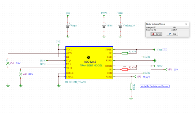
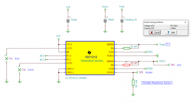
My understanding of SOURCING (CH2) thresholds:

Assuming no RTHR resistor, the ISO1212 has an input threshold of >8.55V ON and < 6.5V OFF referenced to 24V (SENSE2).
I understand this is the ΔV between SENSE2 and FGND2 (in this case, SENSE2 = 24V, so FGND2 needs a low-impedance to GND to pull it's voltage low, generating the needed ΔV.
Correct?

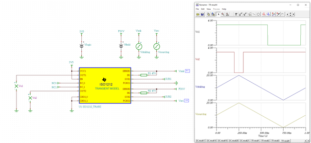
I ask because with the SPICE simulation model, I see the output can go HIGH when the ΔV between SENSE2(24V) and FGND2 is greater than 5V or so.
Is this due to the model's characteristics, or do the thresholds change?

*image removed

  • Hello Katafuchi-san, 

    Your understanding is correct. The VIL with RTHR=0ohms should be 6.5V min for both SINK and SOURCE modes. I suspect that the indicator diode is creating an additional voltage drop and is changing the voltage seen at the RSENSE + LED junction. However, R1 will sink/source ~2.5mA of current (as shown in your measurement) and as long as the current is applied and voltage drop across Rsense is seen this will trigger a high as dictated by the threshold equations in 9.2.1.2.1 Setting Current Limit and Voltage Thresholds. 

    Best,
    Andrew

  • Hi Andrew,

    I'm still not quite sure I understand the behavior...

    In the image I attached, DO24V-1 is 20.4V, and the green LED VF is about 2.5V.

    SINK (Ch. 1)
    You mention for 470Ω RSENSE resistor we expect around 2.5mA, and the simulation shows 2.66mA.
    With this current across a 4.7kΩ resistor, we get a voltage drop of 12.5V. There is a 2.5V drop across the LED.
    So at SENSE1 we get 20.4V - 12.5V - 2.5V = 5.4V.
    This is shown by the VM2 meter blue text in the image.
    Since FGND1 = 0V, and SENSE1 = 5.4V, the ΔV is 5.4V, which is below VIL, and the OUT1 is LOW.
    This behavior is expected, and I understand it.

    SOURCE (Ch. 2)
    However, regarding Channel #2 (SOURCE)
    I have SENSE2 tied to DO24V-1 which is 20.4V.
    FGND has the same LED and 4.7kΩ resistor tied to GND.
    Since RSENSE is the same 470Ω I expect roughly the same current, so 2.66mA.
    If this is the case, there is 2.66mA flowing through LED2 and R7. 
    This means the voltage at FGND2 is 0V + 12.5V + 2.5V = 15V.
    Since SENSE2 is tied to DO24V-1 = 20.4V, then with FGND2 at 15V, the ΔV between these pins is 20.4V - 15V = 5.4V.
    This is shown by the blue text beside the VM1 voltage monitor simulation macro.
    In this case, OUT2 is HIGH, but since the ΔV between SENSE2 and FGND2 is only 5.4V, I expect a LOW, same as the SINK channel.

    My understanding was, the behavior should be the same between SINK/SOURCE, which means with a ΔV of 5.4V, the OUT should be OFF.
    But that is not the case in the SOURCING example.

    You mentioned this being due to the indicator LED and SENSE resistor voltage drop, which I don't understand.
    I believe there was some miscommunication, so hopefully my above explanation helps clarify what I was trying to understand...?

    Thanks!

    Regards

  • Hello Katafuchi-san,

    Thank you for reexplaining. Your questions is clearer to me now. Please allow me an additional day to review with the team and I will get back to you tomorrow. 

    -Andrew

  • Hi Andrew, 

    I don't have access to evaluation hardware at the moment, so I have been tinkering with the simulation model.
    I am back in the office and ran the following test. Much more accurate representation of what I was trying to understand.

    Once channel is in SINKING (FGND1 tied to 0V) configuration, the other is in SOURCING (SENSE2 tied to 20V).
    A variable voltage (0 ~ 20V) is applied to SENSE1 / FGND2 respectively, and a transient simulation was run.

    As you can see, the sourcing configuration, as I understand the implementation, does not follow the ΔV thresholds like the sinking implementation does.

    Is this a simulation artifact, or actual device behavior? (I need to know before I get my hands on some hardware)

    Regards

  • Hello Katafuchi-san,

    Thank you for the clarification and sorry for the delay. The above diagram indicates that the ISO1212 is operating correctly for sink mode. This is okay since ISO1212's input channel is receiving a voltage from a different device. 

    For source mode, the input is providing the 20V to the sensor. Therefore, the source input is meant to be connected to a switch/load. There is no practical reason for the input to see a ramping voltage since a switch would only be open or closed. The correct application would be to short Vsrc to Ground using a switch as you had previously. Vo2 should be 3.3V when the input is shorted. 

  • Hi Andrew,

    Re-did the simulation to avoid voltage sources where they don't make sense.
    Here, I have FGND2 tied to GND through a resistor.
    This resistor represents the resistivity of some sensor.

    As you can see, if the resistor is 6kΩ, the ΔV = SENSE2 - FGND2 = 20V - 15.23V = 4.77V.
    This is clearly below VIL and the OUT2 should be LOW. But as you can see, Vo2 is showing 3.3V.

    Now if we change the resistance to 10kΩ we get the following.
    The ΔV = SENSE2 - FGND2 = 20V - 16.84V = 3.16V.
    This is below VIL and OUT2 is as expected LOW. 
    But the point I am trying to make is the datasheet indicates a VIH of ~8.25V while the simulation is showing OUT2 = 3.3V at 4.77V, which is far below VIL, not to mention VIH. Is this just an artifact of the simulation model, or representative of actual device behavior?

  • Hello Katafuchi-san, 

    I believe this is a possible characteristic of the simulation since the loads used for the sensor are too small in resistance. 

    In source, the standard defines that sensors should consume 2.25mA or less current. Therefore, the R3 resistor which is used to simulate sensor resistance should be increased from 10kohms to 16kohms or higher.   

    Best,
    Andrew

  • Andrew,

    That is what I was wondering. I am working on getting an EVM or two to validate. But I don't see any issues at the moment. I'll open a new thread if anything pops up. Thanks!