ISO7760: ISO7760DW Failure

Part Number: ISO7760

Tool/software:

Hi,

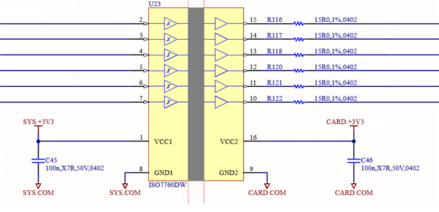
We have a circuit using the ISO7760DW, on two boards we have seen this part fail with the power supply VCC1 shorted to GND1.

Our circuit is straight forward; we are translating 3.3V logic signals across an isolation barrier.

The output drives inputs on an FPGA, the input signals primarily come from 3.3V logic gates. All input signals are referenced to the same rail as VCC1.

We have confirmed no overshoot or over voltage on these input signals.

This has happened on two separate boards on two separate occasions. The boards have not undergone any destructive or stress testing, all testing has been done on a bench or EMC radiated emissions lab.

Any ideas what could be causing this failure?

  • Hello Andrew S.,

    Thank you for the details describing your initial step. 

    "Power supply VCC1 shorted to GND1" is a common failure mode when the absolute maximum conditions are violated. Most commonly, this is EOS on the VCCx pin itself, such as an overvoltage or reverse supply event. Please see the following questions for the next steps: 

    1. Where is the SYS_+3V3 rail powered from? 
    2. Is the supply rail spiking or has an element in the power system (such as an LDO) failed?
    3. Are pins 1-8 connected to an external PCB or is this application all on the same board? 

    Best,
    Andrew J

  • Hello Andrew J,

    SYS.3V3 is generated from a 24VDC to 3V3 Buck Converter based on the LT3971

    We measured all input and power supply signals on start-up, steady-state operation and shutdown. We did not observe any spiking on the power supply rail. The buck converter still seems to be functional after we replace the failed isolator, so I do not believe it to be failing.

    2 out of 6 signals are connected to an external PCB, these are connected to pull-down resistors on the connected PCB. The remaining signals are on the same PCB.

    Thank you for your help,

    Andrew S

  • Hi Andrew S, 

    From the information provided, I do not see anything that would inherently cause a damage to the isolator. Likely, there is some transient or power event from the high-voltage side that is causing damage or a failure after repeated stress.

    My best guess is that the large capacitors on Vout of U38 cause a large inrush current at power on due to high capacitance on the power rail. Managing Inrush Current (Rev. A) may be a helpful application note. However, I am not an expert on the IC used in U38. 

    Best,
    Andrew

  • Thank you for your feedback, Andrew.

    Transients on the 24V side seems unlikely, this has all happened in a lab or workbench setting which should have fairly clean power, we also have upstream transient protection and filtering on our boards.

    I recognise that the buck regulator is an ADI part, and you won't be an expert on it. But it's a fairly typical buck regulator with soft start so initial inrush should be minimal. I also would not expect large load transients on the 3V3 rail either.

    In our testing we have not observed any transients on either the 24V or 3.3V rails

    If you have any other thoughts, please let me know

    Andrew

  • Hi Andrew,

    Please give us an additional day to review and respond.

    Regards,
    Aaditya

  • Hi Andrew,

    Thanks for the patience and sorry for the delay.

    I would like to gain a better understanding of the issue you are experiencing. From my understanding, it seems that the device is getting damaged and causing a VCC to GND short. Is this correct?

    As Andrew mentioned in a previous post, this type of failure typically occurs when there is a high transient or violation of the absolute maximum specifications in some way or form. To get a better idea of your system, can you please provide the following information?

    1. Is there a specific point at which the failure occurs? For example, a nearby switching device, relay, or high power device that operates.
    2. Can you provide the schematic showing the connection to the input and output as well?
    3. Can you also provide a image of the PCB layout of the digital isolator?
    4. Lastly, do you have any waveforms of the VCC1 and VCC1 and signal pins? if not, can you please capture these waveforms at the point where digital isolator starts to fail?

    Regards,
    Aaditya