TPS2663: About reverse polarity protection

Part Number: TPS2663

Hi TI Team,

I noticed in another thread that it is recommended to add a series resistor of $300\text{ k}\Omega$ or higher between IN_SYS and the UVLO/OVP pins to protect them from negative voltage transients.

Following this guidance, I performed some measurements on our board and obtained the following results:

  • When applying -24V to the input: The voltage at the UVLO pin is -0.557V, and the OVP pin is -0.355V.

  • When applying +24V to the input: The voltage at the UVLO pin is 1.42V, and the OVP pin is 0.967V.

The actual resistor values used in my circuit are $R_1 = 750\text{ k}\Omega$, $R_2 = 15\text{ k}\Omega$, and $R_3 = 32.4\text{ k}\Omega$.

The schematic configuration and the definitions of $R_1$, $R_2$, and $R_3$ are shown in the image below:

It appears that the internal protection (such as internal ESD clamping) is functional because the voltages are being clamped. However, even with the $>300\text{ k}\Omega$ current-limiting resistors in place, the measured negative voltages (-0.557V and -0.355V) still exceed the Absolute Maximum Rating of -0.3V specified in the datasheet.

Could you please help clarify the following?

  1. Is this behavior expected when a large series resistor is used to limit the injection current?

  2. Does violating the -0.3V absolute maximum rating under this current-limited condition pose any risk to the long-term reliability of the device?
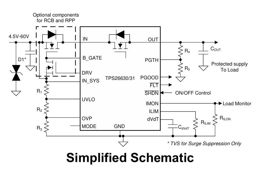
 

image.png

  • Hi,

    Yes, violating the -0.3V absolute maximum rating under this current-limited condition poses risk to the long-term reliability of the device.

    Do one thing generate UVLO & OVLO from VIN which is right after NFET output, this protects the UVLO & OVLO pins.

    thanks,

    Hemanth

  • Hi,

    Thank you for your clear clarification.

    To make sure I fully understand:

    1. Just to confirm, even with the large series resistors limiting the current, the measured negative voltages (down to -0.557V) are considered abnormal/unacceptable and will definitely degrade the long-term reliability, correct?

    2. Regarding your suggestion to "generate UVLO & OVLO from VIN which is right after NFET output", do you mean that $R_1$ should be disconnected from IN_SYS and instead connected to the IN pin (after the NFET)?

      If we change to this configuration, are there any new concerns or design considerations we should be aware of during normal forward operation and reverse-voltage conditions? (e.g., startup delays, NFET gate-drive behavior, or leakage current?)

    3. If we cannot move the detection point to the position after the NFET due to specific system requirements (e.g., we must monitor the input voltage before the NFET turns on), what are the recommended ways to keep these two pins above -0.3V during a -24V reverse input condition?

      Would adding external Schottky clamping diodes (connected from GND to the UVLO/OVP pins) be a viable solution to clamp the negative voltage within the datasheet specification?

    4. If our current hardware design is frozen and no schematic or layout changes can be made at this stage, what would be the immediate risks of leaving it as-is? Will this condition lead to immediate catastrophic failure (e.g., latch-up, physical damage) during a reverse-polarity event, or will it only affect the long-term reliability/lifespan of the device?

    Thanks again for your support and valuable insights.

  • HI,

    1) yes, it will degrade the long-term reliability.

    2) correct.

    3)no that's not a viable solution; it would still affect the reliability.

    4) it will lead to immediate catastrophic failure; device might not start up at all because of internal latch ups  

    thanks,

    Hemanth