ISOW6441: High-frequency noise and interference on low-frequency lines

Part Number: ISOW6441

Hello,

I read the datahseet of the XISOW6441DWER  www.ti.com/.../ISOW6441

and EVM User's Guide: ISOW6441DWEEVM  www.ti.com/.../slvudl7

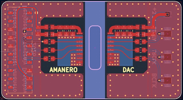
Based on the information provided, I designed my own I2S signal isolator. It receives 3.3V power and BCLK, LRCLK, and SDATA signals from a USB converter (such as an Amanero) and then transmits them— galvanically isolated—to the DAC inputs.

Schematic diagram

PCB Layout

PCB view

In terms of signal transmission, the device works. However, the output signal quality of the ISOW6441 is inferior to the input quality: high-frequency noise and interference from the BCLK signal (frequency range 2.8–12.2 MHz) are superimposed on the WCLK (44.1–192 kHz) and SDATA (frequency range similar to BCLK) signals. On an oscilloscope, this manifests as modulation of the top and bottom sections of the square wave: oscillations appear at the BCLK signal frequency, albeit with a lower amplitude.

Am I right in understanding that this is a manifestation of parasitic capacitive coupling? If so, it is unclear at what level this is occurring—inside the chip, at nearby components, or in the PCB layout —and how it can be eliminated.

 Thank you.

Regards, John D.

  • Hi John,

    Thanks for reaching out.

    The schematic and PCB links shared above are blocked by our internal security team, hence unable to review it. Can you please share those directly here?  - If you're unable to share publicly, then let's connect privately over chat (Sent you the request as well).

    Also, please do share the waveforms clearly showcasing the noise you've mentioned above so that we can better understand the nature of the problem here.

    We need these inputs before jumping into any conclusion and providing further analysis and debug steps. Let us know.

    Regards
    Varun

  • Schematic diagram

    PCB layout

    PCB view

    I didn't take screenshots of the waveforms, but I can do so tomorrow.

  • Hi Dundukov,

    Looks like the Images you tried to share above have not been uploaded properly.

    Regards
    Varun

  • If you're unable to share publicly, then let's connect privately over chat (Sent you the request as well).

    Could you give me a link? It seems none of the ways I use to share images are working for you (even though everything looks fine on my page).

  • Hi Dundukov,

    This is how it looks on my end:

    Just try to paste or drag and drop in this text box - and it should attach the files in the reply.

    We cannot provide any link for connecting on DM chat. You need to accept my friend request and then we can DM each other.

    Regards
    Varun

  • I hope it works this time.

  • Hi Dundukov,

    Yes, I can see it now and have reviewed it.

    Both schematics and PCB Layout looks good - no issues spotted.

    However, I want to confirm one thing since the component designators are not visible - What is the sequence in which C5, C6 and C7 are placed on VISO-GND2? I ask this because I see the order reversed in schematics than what it should be ideally. Can you confirm?

    Also, do share the waveforms so that we can understand what is the nature of the noise and its amplitude that you're observing.

    Regards
    Varun

  • What is the sequence in which C5, C6 and C7 are placed on VISO-GND2?

    In the following order: first 100 nF, then 1 µF, and finally 10 µF, counting outwards from the chip's output.

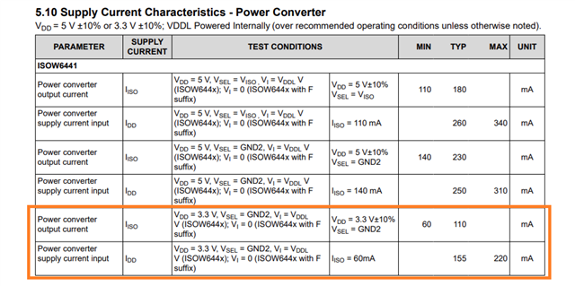
    I noticed that the specifications for the Amanero board (on the signal source side) limit the supply current to 50 mA.

    Is this sufficient for the operation of the ISOW6441?

    The supply current specifications in the ISOW6441 datasheet appear higher; I wonder if the chip is experiencing current starvation.

    This hypothesis needs to be verified.

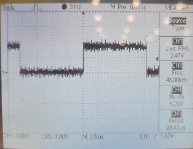
  • The output signal waveforms (for the LRCLK line) are shown below:

    At the same time, the BCLK line frequency was 3.072 MHz. I believe that this is the modulation frequency that is observed, taking into account the resolution of the oscilloscope.

    I also tested the hypothesis regarding the supply current, but it was not confirmed: when using a laboratory power supply instead of the Amanero board, the output signal waveform remained exactly the same. This also made it possible to measure the current consumed by the board—exactly 40 mA—which falls within the permissible limits for the original signal / power source.

  • So, I found the culprit. It turned out to be the ferrite beads in the input and output grounding circuits.

    In the current version of the board, I used Murata BLM18HE152SZ1D ferrite beads (1.5 kΩ @ 100 MHz, 0.5 Ω, 500 mA) - the same ones found on the ISOW6441DWEEVM board. However, they caused modulation of the power ground potential on both sides. I replaced them with jumpers, and all the issues disappeared. This problem was specific to the ferrite beads in the ground path (FB2, FB4); I left the beads in the VCC and VISO paths (FB1, FB3) in place.

    What were the reasons for using them in the ISOW6441DWEEVM?

    I think I need to redesign the board to a version that omits them entirely.

  • Hi Dundukov,

    Thanks for the details above and confirming the capacitor placement. Please find my response below to your questions:

    noticed that the specifications for the Amanero board (on the signal source side) limit the supply current to 50 mA.

    Is this sufficient for the operation of the ISOW6441?

    The supply current specifications in the ISOW6441 datasheet appear higher; I wonder if the chip is experiencing current starvation.

    This hypothesis needs to be verified.

    IDD can be lower in your use case since you are not extracting all of 60mA load current (IISO) out of the VSIO pin. Hence, 50mA is currently enough for your application.

    Also, you confirmed that behavior does not change with lab power supply - May I know what was the current compliance limit set during the connection to PCB?


    What were the reasons for using them in the ISOW6441DWEEVM?

    The ferrite beads were used to primarily block the switching noise from internal DC/DC to propagate on the wider PCB, hence improving radiated emissions performance. You can refer the appnote here - 

    1. Passing CISPR 32 Class-B Radiated Emissions With Ease Using ISOW6441
    2. TI's Latest Signal Isolators with Integrated Power Achieves Lowest Radiated Emissions

    I currently do not have an explanation on why the removal of ferrite bead would help exactly but let me check on this internally.

    Can you let me know where the probing point is on the PCB and how are you probing the GPIO exactly on secondary side?

    1. The reason I ask this is because if passive probe with long leaded ground wires is used then then there's a possibility of radiative noise pickup which affects the signal quality.
    2. This is a technical article which highlights the probing methods and improvements observed - https://www.ti.com/document-viewer/lit/html/SSZTB25

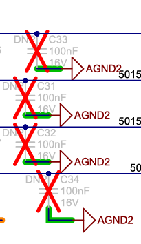
    Apart from removing FB from GND1 and GND2 - there's one more experiment that can be performed which can help in fixing this - this is an option on ISOW6441DWEEVM as well. The below DNP capacitors on GPIO can act as an RC Low pass filter and filter out the high frequency noise.

    Regards
    Varun

  • I connect the probe directly to the U.FL connector: the ground clip to the housing, and the center contact to the solder joint of the U.FL center pin.

    I think, the problem is ground return path interruption. The I2S signals (SDATA, LRCLK, BCLK) operating between the Amanero header, the digital isolator, and the DAC connectors are high-frequency digital signals with fast rise and fall times. High-speed signals require a continuous, low-impedance return path directly beneath or adjacent to the signal traces to minimize loop area. Ferrite beads are designed to introduce high impedance (up to 1.5 kOhm @ 100 MHz) to high-frequency AC signals. Because the ground reference is split by these ferrite beads, on the primary side, the return currents for the signals coming from J4 (AGND1) must pass through FB2 to reach U1's ground (GND1). On the isolated side, the return currents for the signals going to the DAC connectors (AGND2) must pass through FB4 to reach U1's isolated ground (GND2). Forcing high-frequency return currents through the high impedance of a ferrite bead creates a voltage drop across the bead. This results in ground bounce, which distorts the digital waveforms, increases jitter (highly undesirable for audio DACs), and can lead to data transmission errors.

  • Also, you confirmed that behavior does not change with lab power supply - May I know what was the current compliance limit set during the connection to PCB?

    A current limit of 500 mA was set on the lab power supply. The board's actual current consumption was 40 mA.

  • Hi Dundukov,

    Yes, the return current path explanation might be a valid reason here.

    For now, you can go ahead with the design changes above if radiated emissions is not a concern for you. You can also just use a 0ohm resistor by replacing FB2/FB4 instead of redesigning the board, if that is too much trouble.

    We will also work internally to understand this better. Thanks for your interaction and experiments to bring this to our notice.

    Regards
    Varun