ISOUSB111: High power when removing upstream connection

Part Number: ISOUSB111

We have two new designs that are virtually identical other than different mechanical layouts.  We have had a lot of problems in an industrial environment with electrical noise messing up in a big way USB communications to our controller.  We found that using an external isolator that uses the ISOUSB111 worked well, so are now incorporating it into our product.   Of the two layouts, one seems to be working fine, but this is just a sample of one.  The other does not work correctly.  There are two issues which may or not be connected to each other.  The upstream side is powered from the USB +5v power coming over the cable connected to PC port or a USB hub.  Downstream gets it's +5v power from our device.  The USB data ends at a FTDI FT240X USB interface approximately 2" distance away in our product.

  1. If the upstream USB connection is unplugged, the power drain from the ISOUSB111DWXR increases substantially causing the part to get very hot.  How to fix?
  2. Windows recognizes the FT240X USB controller and says it working correctly, even though it is not.  Using the FTDI utility, the FT240 can be accessed and parameters examined.  We tried to change one of the parameters, but when writing the parameter file back out it faulted and the chip went dead.  We had to remove it and reprogram then reinstall.  Fortunately it resides on a daughter board.  We at that point thought the ISOUSB111 was bad and replaced it.  It still came up with the same problems.  Any suggestions on a fix?
  3. We just used the schematic from the TI datasheet.  I looked at other designs and they have series terminator resistors of either 24 or 33 ohms. Should we add these to our implementation?
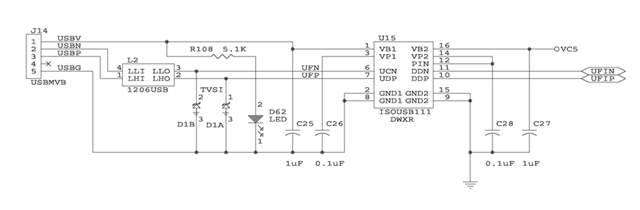
  • Here is the actual schematic.

    ...

  • Hi Thomas, 

    Thanks for reaching out.

    This is an issue that we have never heard of before, hence need your help in understanding every minor detail involved.

    1. We need a rough block diagram on order to understand the full system connection along with the power rails involved to power ISOUSB111 - From Host PC till the last peripheral in the USB chain
    2. Schematic connection for ISOUSB111 that you have designed.
    3. Both the PCB layouts - We need to understand in detail what changes between the two layouts, since one is working fine.
    4. Is the system connection/block diagram as well as all other variables exactly same between the two layouts?
    5. If possible, please insert an ISOUSB111 EVM in between to see if the issue repeats.

    We cannot comment on the FT240 issue you mentioned in Q2 above a we're not the right expert on that. Request you to contact the device manufacturer for right support.

    Also, ISOUSB111 does not require any series resistor on data lines for operation - it's all integrated.

    Regards
    Varun

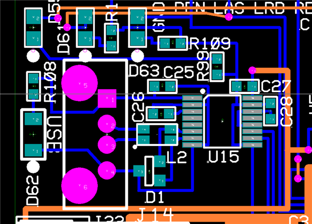
  • There is one big difference between the two on the layout.  The working board

    is a 4 layer board so has a ground plane under everything,  while the faulty board is just a two layer board.  Here is the layout 

    on the two layer board.  In looking it over the layout can be improved by putting a backside layer under the upstream portion

    and connecting it with feedthroughs to the USB ground, and the same on the downstream side connected to our ground.  we are

    in process of layout change to use the correct footprint anyhow.  We don't care about the high voltage isolation, so there are some power/gnd

    traces under the part.

    When these layouts were done, the wrong footprint was used for the part, the regular 16pin ssop.

    So to do our testing we reformed the leads to bend under the part and were able to get a good reflow solder

    connection.

    In answer to one of your questions, the downstream side only goes to the FTDI USB controller.

    On the 4 layer board would you recommend splitting the ground plane and connected the isolated plane to the upstream Ground?

  • Hi Thomas,

    If I've to summarize your inputs above - You say that on the non-working board, the ISOUSB111 was tested on the wrong footprint by pending the pins, correct? 

    If yes, then please know that the whole test is void because the 16 SSOP(DW) and 16 DWX do not have same pinout. Also, in order for us to review in future - I request you to make sure the pin connections are correct.

    Good to see you're going ahead with redesigning the board.

    To answer your question

    On the 4 layer board would you recommend splitting the ground plane and connected the isolated plane to the upstream Ground?

    Your layout inputs above are not very clear here but if splitting ground means splitting GND1 and GND2 on PCB with ISOUSB111 separating them, the yeah this can be done without any issue. You can also refer ISOUSB111 EVM layout as a reference - ISOUSB111DWXEVM Isolated USB Evaluation Module

    Let us know how it goes once your new board is ready.

    Regards
    Varun