Part Number: ISO1212
Hi TI Support,
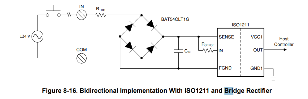
We are using the ISO1212DBQR in our design with the bridge input configuration, similar to the reference circuit shown below (BAT54SW bridge network on both input channels).
Our question is regarding the PCB layout recommendation for the FGND pins (FGND1/FGND2).
In our implementation, the field inputs are connected through the bridge rectifier network, and the FGND nets are not directly tied to the system GND.
Could you please clarify the following:
- Is it recommended to create dedicated copper polygons for FGND1 and FGND2 around the ISO1212 on the PCB, even when using the bridge input configuration?
- Should the FGND polygons remain electrically isolated (floating) except for their intended field-side connections, or is it acceptable to route them as traces only?
- Are there any specific layout recommendations for the bridge input configuration to achieve the best EMC/ESD performance?