Hi,
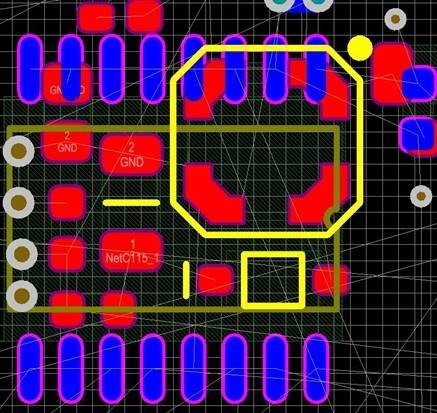
I’m currently working on a new board design that uses TI component ISO3080DWR. Due to tight space constraint, I am considering placing this component on the bottom side of the printed circuit board, underneath the coupled inductor of a Fly-buck type, isolated power converter (using LM25018). The peak switching current through the inductor is relatively small, being 231mApk(max), and the switching frequency is ~370kHz. The converter is used to generate a non-isolated 5V rail, and also an isolated 5V rail from a 36V DC source. I would like to check that the ISO3080 device on the bottom side is not susceptible to magnetic field interference from the coupled inductor mounted above the component on the topside. Could you please give me your views on this?
The following is a view of the board placement as it currently stands. The octagonal shaped component on the top side (in red) is the coupled inductor, and the 16pin SOIC (in blue) underneath it is the ISO3080. The isolation requirements of this design are purely functional only.
Regards,
Deejay


