This thread has been locked.

If you have a related question, please click the "Ask a related question" button in the top right corner. The newly created question will be automatically linked to this question.

ISO7221C: latched 5V output when signal on pin 3 (CH3) is small

Expert 6530 points

Part Number: ISO7221C
Other Parts Discussed in Thread: ISO7721

Team,

We have some problems with ISO7221CD isolator. If signal on pin 3 is around 1.8V/20ns, the output is constant high. Please see below plots.

In other words, small signal on pin 3 (CH3) causes that output (pin 3) latches to 5V until next signal (with larger duration) comes to pin 3.

Customer would expect if signal is too small, output will be 0, and not latched 5V.

Can you advise?

Thanks for your help.

Figure 1 (CH3 Input/CH4 Output)
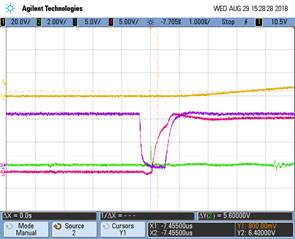
Figure 2 (CH3 Input/CH4 Output)

  • Hi Bartosz,

    The images attached are not very clear and I am unable to identify the channel number in the waveform, can you please share a higher resolution images?
    What was the state of OUTB before and after 1.8V is applied at INB? I believe the waveform answer this questions hence please share higher resolution waveform. Thank you.


    Regards,
    Koteshwar Rao
  • Hi Koteshwar,

    please find attached higher res. scopes in zip below.

    Kind regards

    scope.zip

  • Hi Bartosz,

    Thank you for sharing the original waveform images. I have a few quick questions to understand the situation better.

    1. I understand that CH3 (Purple) is INB (Pin3) and CH4 (Pink) is OUTB (Pin6). Do you know why they are 10V in amplitude? Is that scope probe setting issue?

    2. I see that CH4 is the opposite of CH3 most of the time (especially on image "scope_5.png"), are you sure they are INB and OUTB?

    3. I am still not clear on what issue is customer facing here. Could you please describe again what exactly is the issue?

    I am sorry that I am still not clear on the issue, please help me understand the issue better. Thank you.


    Regards,
    Koteshwar Rao
  • Hi Koteshwar,

    Thank you for your time, let me try to explain the problem in more details.

    We are testing our motor inverter and occasionally, at random (every few to ten seconds), we will get shoot-through problems; both low and high side switch of one of the half bridges gets activated and thus trips desat protection. That happens on all 3 half bridges, also at random.

    After lot of hours of debugging we finally pinned down problem to the ISO7221CD device which is between MCU and gate driver.

    CH1 (yellow) is HV power supply current
    CH2 (green) is the input (PWM) to the ISO (pin3). Output (pin6) of that ISO goes to the gate drive (low side of the half bridge)
    CH3 (purple) is gate voltage - high side
    CH4 (red) is gate voltage - low side

    In picture scope_2 you can see waveforms when everything is normal.
    Pictures 0, 1 and 5 shows fault condition when low side gate CH4 is turned on by PWM duty cycles very close to 0% (CH2)

    From showed pictures you could say that the problem might be in the gate drive, but we saw the output of the ISO and it gets triggered by short impulses, gate drive just follows signal from ISO. Unfortunately, today we saw that we don't have ISO OUT pin6 screenshots and we would have to reassemble test setup to get them, so you need to believe us on this one. :-D

    Like all good HW problems we fixed it in SW by clipping very short duty cycles to 0% and 100% respectively.

    I know that datasheet says min. pulse width 40ns and we are outside that spec. Also, threshold voltage is 2V by DS and our peak barely rises to 1.8V so that might also be a problem, but latched output high is not acceptable behavior in any condition.

    This is just to show you a undocumented problem that caused us a lot of headaches because at first we thought it was a SW problem with PI control loop or with the Timer control unit.
  • Hi Zoran,

    Thank you very much for your detailed inputs in explaining the issue you are facing, appreciate your inputs.

    I understand the problem better now. To summarize the issue, the small 40ns (approx.) pulse at ISO input is causing the low-side switch to turn ON and unfortunately it looks like the pulse isn't turning the switch OFF when it falls back to zero.

    ISO7141 employs an architecture called edge-based architecture where the input data information is transmitted through the isolation barrier only during the input rising and falling transitions. In your use case, it looks like the input rising edge information is transmitted to the output but the input falling edge has occurred too soon to be transmitted to the output. Instead the falling edge information is lost and hence output stays HIGH until the next rising and falling edge transitions happen.

    There are two ways to fix this issue.

    1. Adding an RC filter (with cut-off frequency slightly higher than your switching frequency) at input pins to not pass short invalid pulses through the isolator.
    2. ISO72xx is one of our old digital isolator families released back in 2006. The latest digital isolator family ISO77xx from TI employs a much more robust architecture called On/Off Keying (OOK).

    OOK device transmits input information to the output continuously and not just during the input transitions hence the outputs are much more tightly aligned to their respective input. Even if the output of ISO77xx gets to an error state due to very high CMTI (like 150kV/µs, not easy to create), the output recovers back to the correct state in about 3ns.

    OOK is much more immune to noise and has better overall EMC performance. In addition since ISO77xx input thresholds are CMOS thresholds and not TTL, the input threshold levels are supply dependent and hence provide much higher noise margins. For 5V supply, VIH threshold is going to be >0.7*VCC which is about 3.5V. Thus 1.8V 40ns noise spike will not going to cause a valid HIGH state at the output.

    I would strongly recommend you testing ISO7721 in your application and the issue should disappear with this. Since your application is a motor drive application, I would strongly recommend to use a default LOW state device ISO7721F. When the input signal pin gets floated or input power gets lost, the outputs assume a default state of LOW. This makes sure the motor is stopped immediately under such fault conditions even before the over-current fault is triggered by the gate driver.

    Please do try to test your application using ISO77xx and let us know the feedback. Thank you.


    Regards,
    Koteshwar Rao