This thread has been locked.

If you have a related question, please click the "Ask a related question" button in the top right corner. The newly created question will be automatically linked to this question.

ISOW7842: Layout suggestion

Part Number: ISOW7842
Other Parts Discussed in Thread: ISOW7841

Hi Team,

I received the following request:

##############################################################################################################################
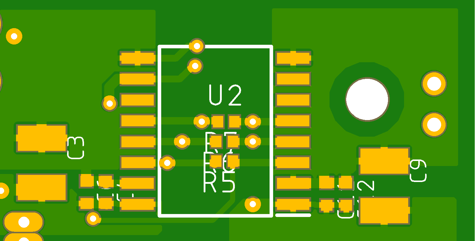
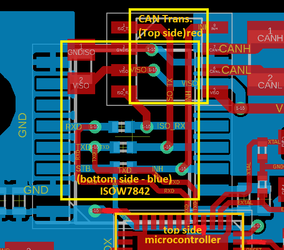
We have a new project focused on isolated can communication. We use ISOW7842 series IC in order to isolate either signals and power.

As an illustration, I attached some images. I have limited size PCB so I arranged ISOW IC (bottom side) and CAN transceiver(top side) as you can see from the attachment. There is also micro-controller next to (below) the ISOW.  My concern is about this arrangement, is it possible to effect the CAN transceiver and micro-controller in terms of electromagnetically (interference) due to DC/DC converter that is inside the ISOW IC ? 

I would like to kindly ask you that do you have a recommendation ? 

##############################################################################################################################

  • Hi Fabio,

    Thank you for sharing the PCB layout for review.
    I understand customer has limited PCB space to place components. Regarding electromagnetic interference of ISOW7841 on other components, I think there would not be any noticeable difference from EMI point of view for the components on the bottom side of the PCB or on the same side. Since the DC/DC converter switching frequency is very high, it shouldn't affect operation of other components on the same PCB layer or on the opposite PCB layer.

    From meeting HV isolation/protection point of view, it is not recommended to have any traces or via in the area between Side1 and Side2 of ISOW. This is especially important for the top and bottom PCB layers which are exposed to air. These traces and via will lower effect isolation voltage, creepage and clearance that can be achieved at system level. Please refer to ISOW7841 PCB layout guidelines in datasheet for recommended PCB layout.

    If your requirement is only to have ground loop separation and do not have EMI immunity requirements like IEC ESD, Surge, etc, then lower creepage/clearance and lower effective isolation voltage might not be a problem.

    If possible, please do share me the schematic of ISOW7841. If it cannot be shared on E2E forum then you can email me the same. Thanks.


    Regards,
    Koteshwar Rao