This thread has been locked.

If you have a related question, please click the "Ask a related question" button in the top right corner. The newly created question will be automatically linked to this question.

ISO7710-Q1: Isolated Inverting Buffer Deterministic Behavior

Part Number: ISO7710-Q1
Other Parts Discussed in Thread: SN74LVC1G14-Q1,

Hi Team,

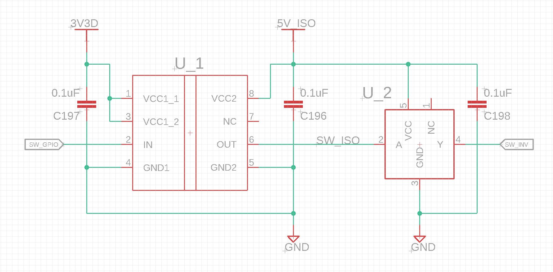
My customer is using an inverting optocoupler device in their design but has run into some issues with the input/output truth table being only valid when the power supply VDD is ready. To combat this problem, they are looking at using the ISO7710-Q1 (F-suffix version) plus an inverting buffer (SN74LVC1G14-Q1) as a functional equivalent circuit .

We'd like to run this circuit by you to make sure it won't cause any unexpected glitches that could mess up the system behavior.

The power sequencing of events is as follows:

  • t=0s - 3V3D is on (3V3D also powers MCU VDDIO)
  • all other power/signal should be low
  • t=100ms - MCU drives SW_GPIO HIGH
  • all other power/signal remain low
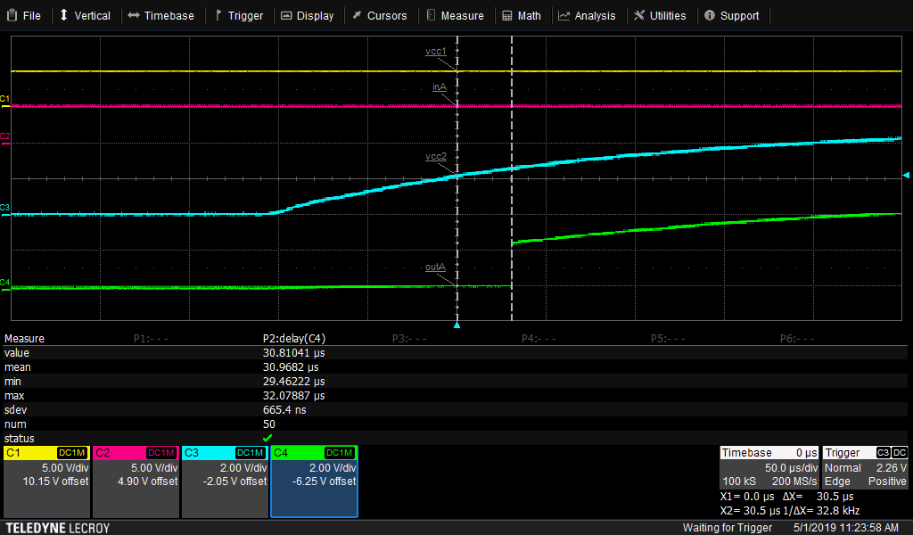
  • t=4s - 5V_ISO is on (5V_ISO is generated by an LDO that is independent of the MCU power supply)
  • expected behavior is that the output of U_1 (SW_ISO) goes from LOW to HIGH immediately because SW_GPIO is held high through out
  • Question: What is the delay between VCC2 going HIGH and OUT going HIGH?
  • expected behavior is for output of U_2 (SW_INV) to STAY LOW during the transition process
  • SW_INV must not be allowed to "glitch" HIGH as 5V_ISO is powered on
  • t=5s - MCU drives SW_GPIO LOW
  • SW_ISO goes LOW
  • SW_INV goes HIGH

Can you please help verify that the above sequence of behavior can be achieved in a deterministic fashion.

  • Question: Are additional PU or PD resistors needed on any of the input or output pins?

Thanks,
Mitchell

  • Mitchell, 

    Great question. Thanks for asking it on the E2E forums. I have some initial thoughts and I may have some more once I can discuss this with the team more next week. 

    First thing: GND1 and GND2 cannot be connected in your schematic. With these connected you are entirely bypassing the isolation barrier. So let's call GND connected to GND1 of the ISO7710-Q1 GND1 and the GND connected to GND2 of the ISO7710-Q1 and the GND of the inverter GND2

    Second: Can we eliminate the inverter altogether by inverting the logic in the MCU? For systems where we are concerned about glitches and startup behavior, generally the fewer the components the better. 

    Now to your questions: 

    In your system, Vcc1 (3V3D) is powered up first and then Vcc2 (5V_ISO). The first issue we run into is that the output of the ISO7710-Q1 is undetermined when Vcc2 is powered down. 

    This can be found in Section 8.4 of the ISO7710-Q1 datasheet on page 17. 

    As look into the Device I/O Schematics this makes sense. The output is truly floating until Vcc2 is above the UVLO (Vcc2 > 2.25V). 

    To make this output deterministic we need to add a weak pull down resistor. The sizing of this resistor is an interesting trade-off. Too much impedance and we have to be concerned about noise, too low impedance and we are constantly wasting too much current. At first pass, I would think a resistor of 100k would probably be appropriate. 

    With this addition of a pull down resistor we now have the deterministic power up sequence we want - but only from the perspective of ISO7710-Q1. I have not yet considered the inverter's behavior. 

    What is the delay between VCC2 going HIGH and OUT going HIGH? - That's a good question. We probably cannot find this number in the datasheet - as the datasheet says the output is undetermined when Vcc2 is unpowered. To understand this number we would probably have to test this on the bench. Is there a particular spec your customer is trying to hit with this question? 

    I'll discuss this more with the team next week to see if we already have some data on this. In the meantime, can you check to see if the inverter is really necessary or can we eliminate it with some change in the code? 

    Have a good weekend, 

    Dan

  • Hi Dan,

    Thank you very much for the excellent details you've provided here.

    Unfortunately, my customer cannot eliminate the inverter stage because it is a fundamental safety mechanism for their system. For this power path management system, they want the MOSFETs to stay on if the MCU crashes or goes into a reset state. Their system uses the TMS570, and in reset the GPIOs on this device default to LOW. With the inverter in place, the default output (under fault conditions) will be HIGH. With that said, it would be great if we could take a deeper look at the inverter's behavior.

    To answer your question on the delay between VCC2 going HIGH and OUT going HIGH, their target is < 100ns.

    Hope you have a good weekend as well. Looking forward to getting some more feedback on this next week.

    Thanks,
    Mitchell
  • Hi Mitchell,

    What if we moved the inverter to side 1 of the ISO7710-Q1? Then it would be powered at t=0, and we could be assured it is inverting the signal as expected for the rest of the sequence.
    If that were the architecture I believe our only concern would be if ISO7710-Q1 can startup with a input driven LOW, and have the output stay low during startup.

    Is this something we could consider?

    Best regards,
    Dan
  • Hi Mitchell,

    I haven't heard from you in a few days. I do have some additional information to share.

    The ISO7710-Q1 would not be able to hit the target of valid output within <100ns of Vcc2 being powered up. I tested this in the lab for one device at room temperature. Over 50 power ups, the average time was 31μs. 

    I'm not sure if this is a deal-breaker for your application. Please let me know either way. 

    Best regards, 

    Dan

  • Hi Dan,

    Thanks for the continued support on this. I really appreciate the heads up. I've talked to the customer about this and we are going to look at moving the inverter to side 1.

    Thanks,
    Mitchell