This thread has been locked.

If you have a related question, please click the "Ask a related question" button in the top right corner. The newly created question will be automatically linked to this question.

ISOW7841: ISOW7841DWER damage question

Part Number: ISOW7841

Hi ti team,

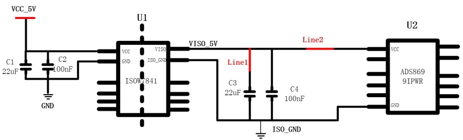
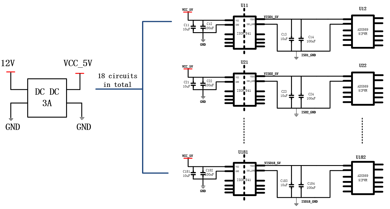
     At present, an isolation chip of TI "ISOW7841DWER" and "ADS8699IPWR" chip are used to complete the isolation voltage collection function. The specific hardware circuit diagram is as follows.5V power supply is provided. During the debugging process, it is always easy to have a short circuit at the 5V power pin of the isolation chip "ISOW7841DWER" near the chip side of "ADS8699IPWR", resulting in abnormal heat of the isolation chip and damage of the chip.

     According to the previous situation, made an adjustment to the circuit, the back-end "ISOW7841DWER" chip capacitor C3 values by 22 uf replacement for 10 uf, "ISOW7841DWER" chip damage problems exist no longer, but using current clamp test, Line1 location, observation by capacitor C3 current waveform that, in the electric moment, through the C3 of around 130 ma peak current, and the chip datasheet above show that chip can withstand 130 ma,

    please help to analyze,Is the chip damaged because the isolated output current is too large?

    which leads to the damage of the internal rectifying current of the chip, short-circuit the output power supply, and is the value of the bearing current on the datasheet available for reference at design ?

Thank you very much!

  • Hi Jimmy,

    Sorry to hear about the issue and thank you for reaching out to us.

    Device ISOW7841 supports 130mA of current when VCC is 5V which is also the case in your application. So 130mA of current will not be the cause of the problem directly. If you have noticed device damage due to overheating then it would probably because of higher output voltage. Please refer to section 11 of ISOW datasheet (Power Supply Recommendations), if the recommendations provided are not followed then there is a possibility for the output VISO to go >8V. This makes device dissipate more power than what it can support even with <130mA of current. Hence, device can get damaged.

    Like it is mentioned in section 11 of datasheet, there are three things that need to be taken care of.

    1. VCC cap should be at least 100µF more than VISO cap.
    2. Input supply current limit should be >600mA.
    3. Input supply rise time (0V to 5V) should be <10ms.

    If the above three conditions are met then you should not see any issue. Please note that not all of the above are necessary for all customers. If customer PCB has decoupling capacitor place farther from device supply pins, then the issue can happen. It can be fixed by simply moving the cap closer to device pins. But if everything is good on PCB and you still see the issue then the above 3 points need to be implemented.

    Hope this answers your question. Thanks.

    Regards,
    Koteshwar Rao

  • Hi,

        My isolation chip isow7841 supplies power to the ADC chip at the back end of the isolation (ADC consumes several milliamperes of current), and also supplies power to the self isolation SPI communication, so the overall power consumption is small. My application circuit uses a DCDC power output of 5V (current output capacity of 3A), which supplies power to the isolation circuit composed of 18 isolation chips. As shown in the figure below is the topology diagram of 18 groups of isolation acquisition circuit after my current rectification. but for the sake of safety, as for the three requirements mentioned in the above email, Some places still need technical help to confirm. The first point is that the end capacitance of VCC_5Vis required to be greater than the end capacitance of VISO 100uF. In my application, the capacity of 18 10uF in the power input pin of the isolation chip in 18 groups of circuits can be equivalent to the capacity of 18x10uF = 180uFshared by all the front power input pin of the isolation chip? Second, the output current capacity of the DCDC power supply is 3A, which does not meet the requirement that the output current of each isolation chip reaches 0.6A, does it have any impact? third, the input and output voltage of the isolation chip are from 0V to 5V, and the rise time is within 7ms, which meets the requirements of less than 10ms. What are the risks if I continue to use my current solution?

  • Koteshwar,

    Could you pls help us check above question,thanks!

         The first point is that the end capacitance of VCC_5Vis required to be greater than the end capacitance of VISO 100uF. In my application, the capacity of 18 10uF in the power input pin of the isolation chip in 18 groups of circuits can be equivalent to the capacity of 18x10uF = 180uFshared by all the front power input pin of the isolation chip?

         Second, the output current capacity of the DCDC power supply is 3A, which does not meet the requirement that the output current of each isolation chip reaches 0.6A, does it have any impact?

         third, the input and output voltage of the isolation chip are from 0V to 5V, and the rise time is within 7ms, which meets the requirements of less than 10ms. What are the risks if I continue to use my current solution?

  • Hi Jimmy,

    Sorry about the delay in my response and thank you for sharing additional information.

    I would like to clarify the requirements to be which I listed in my earlier post.

    1. VCC cap should be at least 100µF more than VISO cap. This is the requirement per device and the caps should be placed close to the device pins.
    2. Input supply current limit should be >600mA. This is the requirement per device, higher inputs minimize the need for this requirement.
    3. Input supply rise time (0V to 5V) should be <10ms. This is the requirement only for the input supply to ISOW, the output is controlled by the device.

    It is difficult to quantify the risks if the above stated conditions are not met but what I would confirm is that meeting these will eliminate the issue. Could you please confirm if I can reach out to you on your email that you have used to create TI account? I can try to understand your application better and try to minimize the needs for above stated conditions. Thanks.

    Regards,
    Koteshwar Rao

  • Hi Jimmy,

    Let me know if I can reach out to you one your email that you have used for E2E? Thanks.

    Regards,
    Koteshwar Rao