This thread has been locked.

If you have a related question, please click the "Ask a related question" button in the top right corner. The newly created question will be automatically linked to this question.

ISOW7842: EMI Issues

Part Number: ISOW7842
Other Parts Discussed in Thread: ISOW7841,

Hello,

I have a design using the ISOW7842.  I followed the guidance in SLLA368C "Low-Emission Designs With ISOW7841 Integrated Signal and Power Isolator"  However the design is failing FCC Class B

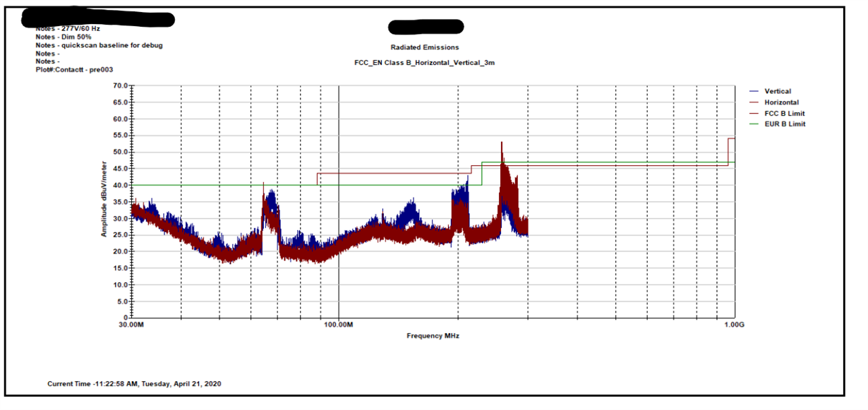
I was able to add an inter-plane capacitance of about 20pF.  This is the 2nd scan of the device and was a quick scan from 30-300Mhz.

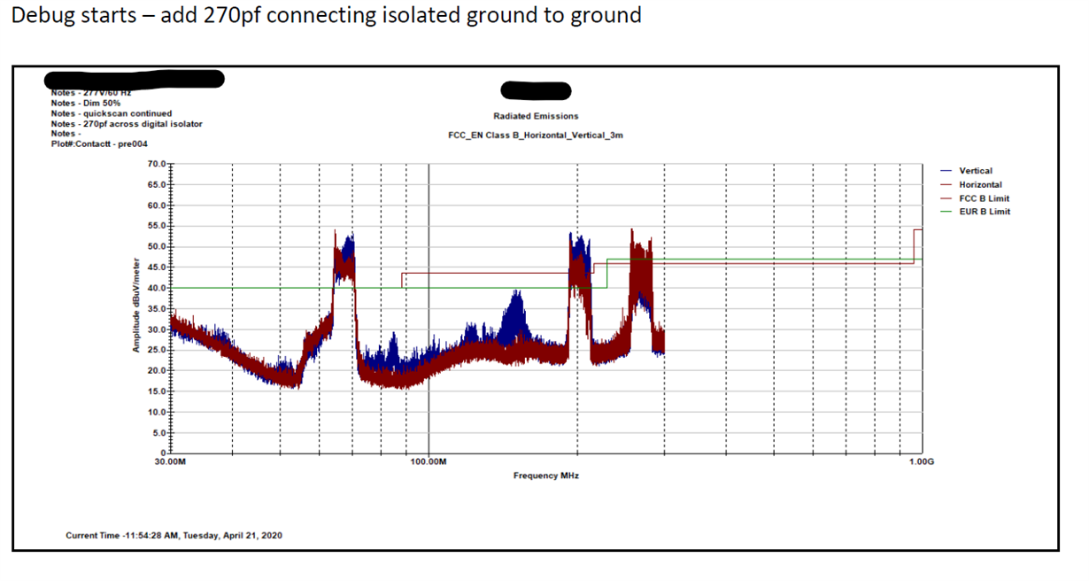
Here is the 3rd scan with a 270pF capacitor soldered across the grounds of the isolator.  As you can see...this only made things much worse.

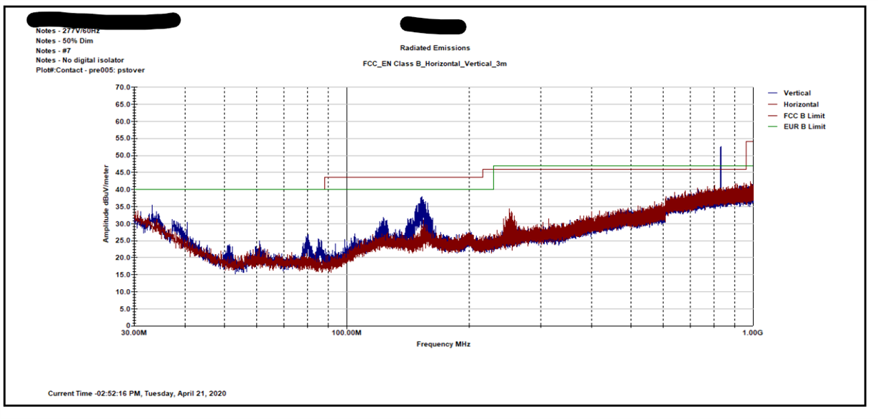
Here is the scan without the isolator IC removed from the board.

Please let me know your thoughts on this.  I would able to share more information in a non-public forum.

  • Hi Jason,

    Sorry to hear about the issue and thank you for sharing the emissions results to understand your current situation.

    Looking at the results, I see that you need about 10dB or more improvement to comfortably meet the requirement. I understand that you already have an inter-layer capacitance of 20pF implemented. It definitely helps to have this inter-layer stitching capacitor to significantly reduce radiated emissions, though 20pF of capacitance is usually not sufficient to meet requirement emissions requirements. Do you think you will be able to further increase the capacitance? Maybe by reducing the distance between the overlapping layers which is the capacitance thickness. If you can achieve 50pF of capacitance, then I am confident the emissions results are going to be much below the Class B limits.

    Using a physical capacitor (Y-cap) connected between the two sides of isolator may produce improvement but is largely dependent on how this is positioned on the PCB. Like it is described in the App Note SLLA368, the physical capacitor introduces lead inductance due to the connections in addition to its own parasitic inductance. This capacitor should be placed as close as possible to device pins (maybe GND1-GND2) to see an improvement. It is also important to note that the improvement from Y-cap is going to be limited due to the unavoidable parasitic inductance.

    If increasing the stitching is not an option, then using a CMC on both sides of supply pins is going to bring significant improvement.

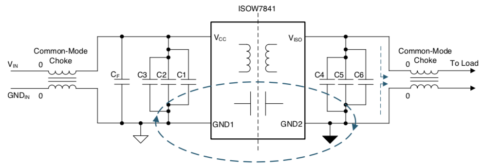
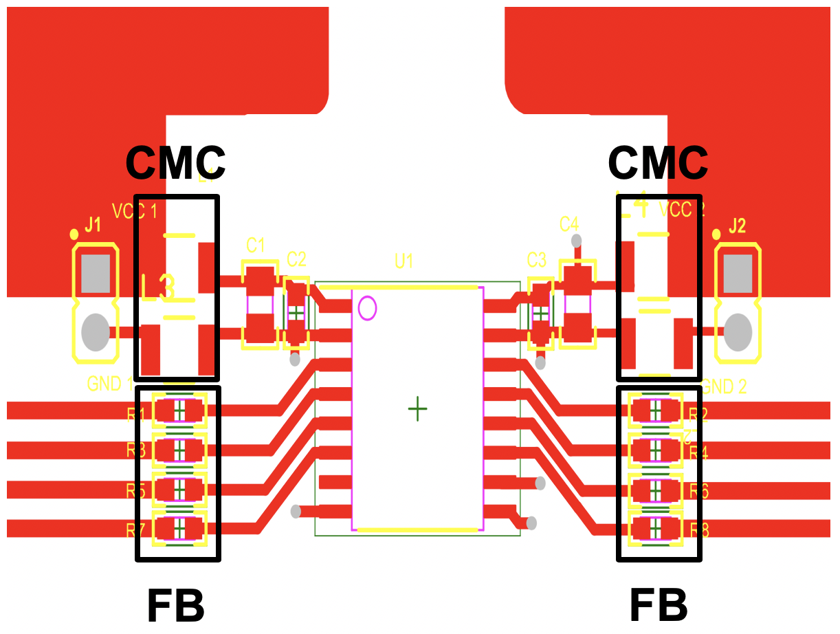
    1. Common-mode chokes (CMC) to be used on both VCC/GND and VISO/GNDISO and the way shown in below schematic and PCB layout.
    2. Please note that the CMCs to be chosen such that the impedance of CMC is >>1kΩ at the frequency points where emissions are observed.  We expect the emissions at ~60MHz to be prominent compared to other frequencies, hence, I recommend below the two CMC part numbers.
      1. CMC - 200mA, 15kΩ - TDK - ACT1210-510-2P
      2. CMC - 200mA, 20kΩ - TDK - ACT45B-510-2P
      3. CMC - 200mA, 10kΩ - Wurth - 744235510
    3. The I/O lines can have resistors (>1kΩ) instead of ferrite beads (FB).

    Regards,
    Koteshwar Rao

  • Thank you!  This is excellent information! 

    1) I'm good adding the common mode chokes.  I just don't have any more square inches for inter-plane capacitance and I'm already at 4.8mil between the two layers and I have 6KV surge to worry about.  ISOLA 370HR is 1350V/mil and I have 4.8mil, puts me right at 6480V.

    2) Are the series FB or 1K resistors necessary if my communication rates are low (56Kbps) ?  Or will each line radiate if it is logic "High"?

    3) WRT, capacitances, I think there should be 1000pF and 100nF and 1uF for the capacitances on either side.  The 1000pF is the only capacitor that isn't inductive at 100Mhz.  Thoughts?

  • Hi Jason,

    Thank you for your quick inputs.

    • I understand. Seeing your 6kV surge requirement, I recommend another approach. Apart from building a board with both inter-layer stitching cap and CMCs, you could also build another variant of PCB that only CMCs and no stitching cap. If the second PCB already meets your emissions requirement, then you don't have worry about surge performance at all.
      • The thickness between the overlapping layers may or may not be very well controlled by the PCB manufacturer. This may cause the isolation performance difference from PCB to PCB. Hence, when actual isolation levels are critical it best to see if the emissions can be met without the stitching cap and hence my recommendation of also building the second PCB with only CMCs.
    • The FB/1kΩ resistor recommendation is independent of the actual datarate or state of I/O pins. This is more to do with common-mode radiations from the DC/DC converter in ISOW device. Since the data isolation channels share the same GND with power supply, it is also important segregate the I/O lines also from rest of the PCB just the way CMCs are doing to the power supply lines.
      • We do not see any significant impact on radiations due to usage or non-usage of I/O lines radiation filtering, but it is always recommended to leave a footprint to be able to test if needed. After the testing, you can always take a call of what to retain and what not to.

    • Regarding the decoupling capacitor recommendation, we recommend at least 10µF + 0.1µF capacitor at both input and output supply pins. Any additional capacitance at the input supply pins is always beneficial.

    Regards,
    Koteshwar Rao