This thread has been locked.

If you have a related question, please click the "Ask a related question" button in the top right corner. The newly created question will be automatically linked to this question.

ISO7741: Output Behavior

Part Number: ISO7741

There is a question about the output behavior with Input and power supply. 

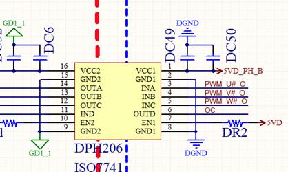
There are some test with ISO7741 here. 

Conditions: VCC1 is floating (DC49,DC50 are not populated on the PCB)

Test 1: When INA, INB, INC are supplied by 5V,there is about 4.2V voltage can be seen between VCC1 to GND1.

Test 2: When INA is low logic,and both INB and INC are supplied by 5V,there is about 4.2V voltage can be seen between VCC1 and GND1. 

Test 3: When INA and INB are low logic, and INC is high logic with 5V, the voltage between VCC1 and GND1 is continue changed in 0V to 4.2V.

Test 4: When INA and INB are low logic, and INC is low logic, there is 0V between VCC1 and GND1. 

With above measurements, is this behavior normally? Could you explain why he behavior are? Very thanks. 


  • Hi Brian,

    Thanks for reaching out. Please see my inputs to the test conditions you have listed out.

    Test 1: Since there is a ESD bypass diode between INx and VCC1, the device gets powered when at least one of the inputs is HIGH provided there is sufficient current sourced by the device connected to INx (like MCU). Since device is indirectly powered, all outputs will follow all the inputs assuming VCC2 is also powered.
    Though this is expected, operating in this condition affects device reliability. The ESD bypass diode is only designed to support ESD pulses that last only a few 10s of nanoseconds and not continuous current.

    Test 2: Since there is a ESD bypass diode between INx and VCC1, the device gets powered when at least one of the inputs is HIGH provided there is sufficient current sourced by the device connected to INx (like MCU). Since device is indirectly powered, all outputs will follow all the inputs assuming VCC2 is also powered.
    Though this is expected, operating in this condition affects device reliability. The ESD bypass diode is only designed to support ESD pulses that last only a few 10s of nanoseconds and not continuous current.

    Test 3: Since there is a ESD bypass diode between INx and VCC1, the device gets powered when at least one of the inputs is HIGH provided there is sufficient current sourced by the device connected to INx (like MCU). Since device is indirectly powered, all outputs will follow all the inputs assuming VCC2 is also powered.
    Though this is expected, operating in this condition affects device reliability. The ESD bypass diode is only designed to support ESD pulses that last only a few 10s of nanoseconds and not continuous current.

    Test 4: Since all the inputs on VCC1 side are LOW, the device doesn't get powered. Hence, all the outputs will go to default state provided VCC2 is powered.

    We do not recommend powering the device through input pins. Thanks.

    Regards,
    Koteshwar Rao

  • Thanks Kote for detailed comments.