Hi,
My customer has questions about TPS7B770x-Q1.
Could you tell me about questoins?
[Question]
- Is there Dropout Voltage vs Output Current Characteristic at Tj=85C?
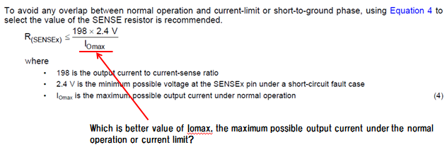
- If my customer sets Vsense=2.4V that is the maximum possible output current under the normal operation, how much is the Vsense voltage between normal current and over currnet?

- How much is the delay time of Vsense output after detecting overcurrent?
Best Regards,
tateo