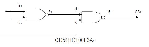
As shown in figure, we use the first NAND gate of CD54HCT00F3A to receive signal(width of 1.6 u s, voltage of 4.8 V pulse signal), pin 5 always at 5 V high level, the output of the second NAND gate as a chip select (Low Level effective). we use the signal generator to produce signal (frequency of 312.5 KHz) to pin 1, the pin 6(CS)should be output 312.5 KHz low level, but it always at a high logic level with an oscilloscope observation . Adjust the signal generator produce frequency to 2 KHz and below, the output of pin 6 (CS) is normal. In addition, Through the oscilloscope observation ,the output of pin 3 is nomal. what may cause to this failure?