This thread has been locked.

If you have a related question, please click the "Ask a related question" button in the top right corner. The newly created question will be automatically linked to this question.

SPI DMA reads incorrectly on TMS470R1B1M

Other Parts Discussed in Thread: ADS1278, TMS470R1B1M, SM470R1B1M-HT

Hi, 

I have a SPI-DMA setup on TMS470R1B1M to fetch data from ADC (ADS1278). This is a 24bit ADC and there are 8 channels. So we read 24 bytes on every ADC cycle. It reads good data but once in a while on power up it starts reading bad values. I have a constant voltage fed to ADC channels. When it reads the bad values, the values jump all over the place. After some debugging I realized that the first byte is some bad value but then the rest of the data corresponds to the good data bytes, but now everything is offset by 1 byte in the array due to the first bad data byte. Also the last byte is lost. I verified that the ADC is sending good values as I gather them on scope. I see that it is sending good packets over SPI. My conclusion is that the DMA is the culprit which somehow does not increment the destination address properly.

Any idea what could be going wrong. I tried to halt the DMA (which should reset the internal regs, but this did not help. 

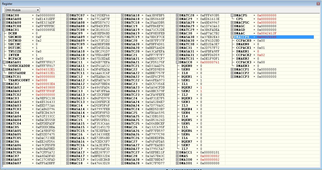
My DMA setup is as follows:

******************* DMA Setup ******************************

// DMA setup for SPI1:RX (Packet 1/Channel 1)
// Control Packet 1 Configuration
DMAC01 = 0 | TRSIZE_0 | INTEN | DSTINC | DSTMOD_2 | SRCMOD_15;
DMASA01 = (uint32_t)&SPI1BUF + 3; // Interested in the Lowest Byte so skip first 3 bytes (SPIBUF is 4 bytes)
DMADA01 = (uint32_t)rxbuf;
DMATC01 = 24;
// Notify the DMA that Control Packet 1 is updated
DMACPS |= CPACK_1;
// Channel 1 Configuration
DMACC0 |= SEN1 | RQEN1;
// Channel 1 Enable with Control Packet 1
DMACCP0 |= CCPACK1_1 | DMEN1;

// DMA setup for SPI1:TX (Packet 2/Channel 2)
// Control Packet 2 Configuration
DMAC02 = 0 | SRCINC | SRCMOD_2 | DSTMOD_15;
DMASA02 = (uint32_t)txbuf;
DMADA02 = (uint32_t)&SPI1DAT0 + 3; // 1;
DMATC02 = 24;
// Notify the DMA that Control Packet 2 is updated
DMACPS |= CPACK_2;
// Channel 2 Configuration
DMACC0 |= SEN2 | RQEN2;
// Channel 2 Enable with Control Packet 2
DMACCP0 |= CCPACK2_2 | DMEN2;

****************************************************************

byte rxbuf[24], txbuf[24];

************** SPI-1 Init *****************************************

// Enter SPI reset mode
SPI1CTRL2 &= ~SPIEN; // Place SPI in reset
SPI1CTRL3 &= ~RX_INT_EN; // Disable SPI receive interrupts

// Configure SPI port 1
SPI1CTRL1 = 0 | CHARLEN_8; // 8 bits/char

SPI1CTRL1 |= SPI_PRESCALE_47; // ADC Clock = 1 MHZ

SPI1CTRL2 |= MASTER; // We are the master
SPI1CTRL2 |= CLKMOD; // We drive the clock
SPI1CTRL2 &= ~POLARITY;
SPI1CTRL2 |= PHASE;
SPI1PC6 = 0 | CLK_FUN; // SCLK pin
SPI1PC6 |= SIMO_FUN; // SIMO pin
SPI1PC6 |= SOMI_FUN; // SOMI pin
SPI1CTRL3 |= DMA_REQ_EN; // DMA request enable
SPI1CTRL2 |= SPIEN; // Activate the SPI

************ DMA Init *****************************************

DMAGC = 0; // Channel service size = 1
DMAGD = 0; // Clear STOP and HALT mode
DMACPSCLR = 0; // Disable all control packets
DMAS = 0; // Clear all pending interrupts
DMACCP0 = 0; // Disable channels 0-3
DMACCP1 = 0; // Disable channels 4-7
DMACCP2 = 0; // Disable channels 8-11
DMACCP3 = 0; // Disable channels 12-15

************************************************************

I would appreciate some help on this. 

Pinakin 


  • Pinakin,
    I will take a look at this and see if I can spot any issues.
    Regards,
    Wade
  • Thanks Wade. Let me know if you need to know any more info from my end.

    Pinakin
  • Pinakin,
    Could you share the schematic connections from ADC to R1B1M?
    Also, what is order of execution of above setups?

    You can reference the SPI DMA examples here. www.ti.com/.../toolssoftware
    It is in the "SM470R1B1M-HT CAN SPI Driver" After installing, you can reference files in \examples\SPI\Src and in doc directory.
    There are specific comments related to the order in which spi and dma is enabled.

    Regards,
    Wade
  • Wade,

    Here is the snapshot of the schematics SM470R1B1M___ADC1278_schematic.pdf 

    Here is how the ADC setup works:

    The ADC DRDY triggers an interrupt when the ADC conversion is complete - indicating that the data can now be fetched by controller. This will setup DMA to perform the ADC data fetch over SPI (DMA setup is shown in my first message above). The DMA will fetch the data and on completion will trigger another interrupt indicating the other modules in firmware that the ADC data is ready for use.

    I have looked at the example (you specified) before. Do you see anything incorrect with my code? Let me know if you have any suggestions for the code. 

    Thank you, 

    Pinakin 


  • Pinakin,

    So just based on this:

    "It reads good data but once in a while on power up it starts reading bad values. I have a constant voltage fed to ADC channels. When it reads the bad values, the values jump all over the place. After some debugging I realized that the first byte is some bad value but then the rest of the data corresponds to the good data bytes, but now everything is offset by 1 byte in the array due to the first bad data byte. "

    I doubt very much that the issue is your DMA configuration... at least directly. That's not something that would normally cause a symptom like 'works most of the time, but sometimes on power up the first byte is bogus'.

    The likely root cause of such an issue would be something like one of the ideas in this list. Check "F" first though.

    a) power up timings. you have 2 chips that you are interfacing. each may need some time on power up to initialize.
    could it be that you are trying to access the ADC chip before it's ready, causing the initial garbage data.
    I would check the datasheet of the ADC chip to look for any parameters that may indicate it needs time after power up
    before it can respond to SPI commands.

    b) pin states during reset, pullups, pulldowns, etc.
    I would scope the control signals to the ADC during a power up and see if perhaps due to pullups, device initialization code,
    or some other transient reason you are seeing something that would cause the ADC to make a bogus conversion.
    I don't know what 'triggers' the ADC but perhaps it's something like a 'low' on chip select and maybe this occurs
    during power on just because of the default state of pins and pullups/pulldowns.

    c) order of DMA requests. make sure that the receive event is actually triggering the DMA that causes the read from SPIBUF & write to RAM. if somehow this is triggered by RXRDY by mistake, then

    d) DMA channels being shared. check the datasheet for the DMA requests ... many times the DMA request line is shared among several peripherals. make sure any other peripherals on this request like are dormant and not causing

    e) make sure that there isn't a bogus DMA request detected by the INT pin during power up. you don't want it to
    just see a pullup or pulldown resistor w. slow rise time and consider this a 'request' from the ADC.
    Before enabling the DMA request you may want to make sure there's not one already pending.

    For this potential problem (e) you can scope out the timing of the ADC's /DRDY with respect to the SPI clock to look for the case where the SPI may be triggering before a 'real' /DRDY fromt he ADC.

    It would be great if you can 'control' the ADC's conversions starting / stopping. If it just starts automatically by itself then you may need to clear the first /DRDY interrupt during power up if it's bogus due to a rise or fall on INT1 that's occurring during power up.

    f) similar to "E" but our chip may generate a DMA request if you have an input that is 'high' and then you change the polarity of the edge detection from rising to falling. I believe that it may just 'invert' the input signal which would make it look like a edge when there isn't one. If this is the case, clear that bogus edge detect after setting the polarity and then enable the DMA request.


    Otherwise your DMA control packet 'looks' right. To confirm I would want to know the hex addresses to which everything resolves to make sure it's not some C code pointer problem but if you say it's working most of the time then I don't think it's a problem here.
  • Anthony,

    I have looked at the scope outputs on DRDY line and the DMA request ISR. When DRDY occurs it triggers DMA request. Once DMA is complete it triggers DMA ISR which then buffers the fetched ADC data into a separate buffer for processing later on.

    a) If there is power up sequence issue then the first few readings on ADC would be bad but then eventually it will catch up and show good values; but I dont see this behavior so I dont think this is the issue.
    b) Again this issue continues after power cycle until the power is cycled. Also the chip select on ADCs are pulled low on hardware as we have dedicated a SPI bus only for ADC. So I dont think this is the cause.
    c) The way I have configured this is that when DRDY on ADC goes low it triggers an interrupt, which then sets DMA to fetch data from SPIBUF. Do you see any issue with this?
    d) In my project only one of the SCI ports use DMA for RX and I verified that it uses different packet and channel. So this should not be an issue.
    e) I have verified that the DMA completes well before the next DRDY occurs. Also when I managed captured this problem with the JTAG, I noticed that the data was good but shifted by 1 byte. The first byte was garbage value and the next bytes were actually good ADC vaues. So I dont think that it was a bogus DMA request - also DMA is configured to fetch data based on DRDY line on ADC chip. My concern is when I managed to catch this issue in action I noticed that the first byte was garbage. I dont know if there could be a situation where there can be multiple garbage values before I get good valid ADC data.
    f) SPI and DMA initialization is done at power up. So I dont expect a edge detection change halfway in between ADC data fetching.

    Here is code snippet I am using.

    /* -------------- INITIALIZATION -------------- */
    /* SPI */
    void Init_SPI(void)
    {
    // Enter SPI reset mode
    SPI1CTRL2 &= ~SPIEN; // Place SPI in reset
    SPI1CTRL3 &= ~RX_INT_EN; // Disable SPI receive interrupts

    // Configure SPI port
    SPI1CTRL1 = 0 | CHARLEN_8; // 8 bits/char
    SPI1CTRL1 |= SPI_PRESCALE_7;
    SPI1CTRL2 |= MASTER; // We are the master
    SPI1CTRL2 |= CLKMOD; // We drive the clock
    SPI1CTRL2 &= ~POLARITY; // CLK Polarity = 0
    SPI1CTRL2 |= PHASE;
    SPI1PC6 = 0 | CLK_FUN; // SCLK pin
    SPI1PC6 |= SIMO_FUN; // SIMO pin
    SPI1PC6 |= SOMI_FUN; // SOMI pin
    SPI1CTRL3 |= DMA_REQ_EN; // DMA request enable
    // Exit SPI reset mode
    SPI1CTRL2 |= SPIEN; // Activate the SPI
    }

    void Init_DMA(void)
    {
    DMAGC = 0; // Channel service size = 1
    DMAGD = 0; // Clear STOP and HALT mode
    DMACPSCLR = 0; // Disable all control packets
    DMAS = 0; // Clear all pending interrupts
    DMACCP0 = 0; // Disable channels 0-3
    DMACCP1 = 0; // Disable channels 4-7
    DMACCP2 = 0; // Disable channels 8-11
    DMACCP3 = 0; // Disable channels 12-15
    }

    void Init_IRQ(void)
    {
    REQMASK = 0; // Disable all interrupt request channels
    REQMASK |= (1 << (int32_t)CIM_GIOA); // Enable GIO channel
    ...
    }
    /* -------------------------------------------- */
    /* -------------- Interrupts --------------*/
    __irq __arm void IRQ_Handler(void)
    {
    switch ((0xff & IRQIVEC) - 1)
    {
    ...
    case CIM_DMA0 : DMA_IrqHandler(); break;
    case CIM_GIOA : GIOA_IntHandler(); break;
    ...
    }
    }

    void GIOA_IntHandler(void)
    {
    // Process high priority first
    switch(GIOOFFA) // reading register clears GIOFFA and corresponding bit in GIOFLG
    {
    case 0: break; // no high priority irq to handle, BREAK and check low priority
    case A1: // high-level interrupt 1 from the external ADC's (nDRDY)
    // Begin transfer of the current ADC sample into the receive buffer
    SPI1_DmaExchange();
    return;
    }
    }

    /* -------------- This sets up DMA to fetch ADC data -------------- */
    void SPI1_DmaExchange (uint8_t *txbuf, uint8_t *rxbuf, uint16_t size)
    {
    // DMA setup for SPI1:RX (Packet 1/Channel 1)
    // Control Packet 1 Configuration
    DMAC01 = 0 | TRSIZE_0 | INTEN | DSTINC | DSTMOD_2 | SRCMOD_15;
    DMASA01 = (uint32_t)&SPI1BUF + 3; // Interested in the Lowest Byte so skip first 3 bytes (SPIBUF is 4 bytes)
    DMADA01 = (uint32_t)&rawAdcBuffer[raw_Buf].raw[0];
    DMATC01 = size;
    // Notify the DMA that Control Packet 1 is updated
    DMACPS |= CPACK_1;
    // Channel 1 Configuration
    DMACC0 |= SEN1 | RQEN1;
    // Channel 1 Enable with Control Packet 1
    DMACCP0 |= CCPACK1_1 | DMEN1;

    // DMA setup for SPI1:TX (Packet 2/Channel 2)
    // Control Packet 2 Configuration
    DMAC02 = 0 | SRCINC | SRCMOD_2 | DSTMOD_15;
    DMASA02 = (uint32_t)txbuf;
    DMADA02 = (uint32_t)&SPI1DAT0 + 3;
    DMATC02 = size;
    // Notify the DMA that Control Packet 2 is updated
    DMACPS |= CPACK_2;
    // Channel 2 Configuration
    DMACC0 |= SEN2 | RQEN2;
    // Channel 2 Enable with Control Packet 2
    DMACCP0 |= CCPACK2_2 | DMEN2;
    }


    Please let me know if you see any issue with this.

    Regards,

    Pinakin
  • Hi Pinakin,

    I probably misunderstood the 'on power on' condition.

    I don't see a problem in your code. If you want us to make a more careful assessment of it please provide the hex values that wind up being written to the DMACP2. "symbolically' they look ok but sometimes there could be an issue int he #define or in the way the code is compiled.. And it's ultimately the hex values that the DMA will respond to.

    But given that DMA configuration looks ok and it works most of the time, with only occasional failures. my instinct is to look outside this area. If you run for any significant time I think you must be cycling through the DMA CPs many times successfully and only occasionally 'missing' but let me know if this is wrong.

    Have you confirmed that there isn't any sort of noise or glitching on the DRDY/ ? What is the risetime of this signal?
    If it's not fast I might be concerned.

    The R1B1M is also a distant memory to me but are you using any other GIO in the same module to generate interrupts?
    If so can you correlate the corruption with activity on the other GIO channel?

    One other idea - how are you resetting the DMA CP's to keep this running continually? Is a CPU interrupt being used or are they auto-initializing themselves? If there is a CPU interrupt involved, we need to consider the possiblity of some sort of ordering or interrupt priority issue being the culprit.

    Best Regards,
    Anthony
  • Anthony,

    I am confused. Why is there a need to cycle through DMA CPs. I always use channel 1 packet 1 for SPI Rx - to fetch ADC data) and channel 2 packet 2 for Tx (which is dummy data). I know for sure that DMA completes before next DRDY. So I reuse the same channel/Packets for SPI.

    Also I am not sure what is DMACP2 hex value. I dont see any such register. I tried searching for it as well in code. I dont see any #define for it.

    Pinakin
  • Anthony,

    Also I verified DRDY and it looks good. Here is a snapshot of the scope. The top blue waveform (sorry the scope colors are not greatly visible) is DRDY. The yellow indicates DRDY triggered ISR which sets up DMA and does some buffering related stuff. The purple wave indicates end of DMA fetching.

    Pinakin


  • Hi Pinakin,

    The waveforms look almost 'too good' but I don't know what the timescale is either.
    What we need to see is a zoomed in view of the rising edge on the blue waveform.
    Would like to know if the risetime is 1ns, 10ns, 100ns, ... for example.

    Regarding the hex values - please with a debugger attached run to the code that writes the control values into the DMA RAM.
    Then just tell us exactly what values are being written. If you have to, you can open a register view and step through the code that does the write, you'll see something like str rx, [ry + #offset] or something and rx, ry will be registers.
    The value to be written will be the contents of the register 'rx' in that case.

    What I meant by the DMA recycling is this - there isn't infinite RAM so if you are continually running conversions you must have a circular buffer implemented. The DMA can accomplish this by auto-initializing the control packet after it completes... for example when it finishes all of the count (size) it can reset it's pointers back to their initial state (back to the start of the buffer) and continue transferring. If it's not auto-initializing then it would rely on your code to reset the control packet.

    Either way though I guess this points to another way your program might fail - that is synchronizing between the DMA and the CPU.

    I believe we had interrupts at the 'block half complete' boundary so that you could process half of a block while the DMA still had half the block left to put new incoming data into. This gives time for interrupt latency.

    If you arent' using this type of interrupt but instead are using the block complete interrupt ... then maybe if the DMA auto-initializes it could be writing over the first byte of the buffer before your CPU can read it.

    So let's say your size = 'N' then instead of sample # m*N the CPU might be reading sample #(m+1)*N which would look out of sequence if you have assumptions of your waveform. This would be a possibility if you interrupt say at the end of the block transfer and the ISR starts reading data from the beginning of the block. If the interrupt latency of the CPU gets larger than one ADC sample time for some reason [e.x. higher priority interrupts block the DMA interrupt] then the incoming SPI data could overwrite the previous data before the CPU reads it.

    So maybe what we need to know as well is what is your strategy for circular buffering and where do you interrupt?
  • Hi Anthony,

    Here is the screenshot of the registers. 

    I dont see any values incorrectly displayed here. Also if there is an issue with this then I should never be getting good values, right? 


    I captured the DRDY pulse. Here are the screenshots with the rise/fall timings. Please refer to the zoomed images for accuracy. 

    I would say fall time is ~ 15 ns and rise time is ~ 9.6 ns. 

    Pinakin 


  • Hi Pinakin,

    Ok then for now I would say look elsewhere. I don't completely understand the DMA control packet (haven't decoded it) but if it's working most of the time and if you see what you expect in the register window that's good enough. Unlikely this is the issue anyway.

    The rise/fall times look ok too. 10-15ns is on the slower side of what I'd like to see but I think the interrupt line is sampled by the internal clock and so it should be fine with a 10-15ns edge.

    Next thing to understand clearly is your buffering scheme. Are you interrupting the CPU at the 1/2 buffer full boundary?
  • Anthony,

    I buffer data in 2 buffers. Buffer-1 and 2 alternately collect ADC data. While one buffer collects data thee other is being processed. This way there is not conflict in the data that is processed.

    Pinakin
  • Hi Pinakin,

    Ok. But then how do you switch the DMA over from one buffer to the other? (Since the buffer pointer is contained in the control packet)..
  • Anthony,

    I did some time profiling on this. The time required for buffer processing is about 120 us. The ADC DRDY signal comes every 2.56 ms. So there should be no conflict, right? Also when DRDY triggers ISR it sets up DMA with the pointer to the buffer that is ready.

    Pinakin
  • Hi Pinakin,

    To understand better -

    1. ADC DRDY fires every 2.56ms.

    2. This triggers 1 DMA transfer RAM to SPI TX

    3. SPI RX Ready triggers the DMA transfer from SPI to RAM

    4. When the DMA control packet completes 'size' of these transfers, you trigger an ISR

    5. In the ISR the CPU processes the data and resets the DMA controller to the 2nd buffer area

    Is that about right? (Especially not certain about step #5.

    What would (possibly) concern me is that even if the processing only requires 120ms - if something were disabling interrupts [like a higher priority interrupt, FIQ, OS critical section] could it ever disable interrupts for longer than your 2.56ms and then you miss setting up the DMA control packet in time for the next data.

    Such an affect would show up by having your corruption appear at some multiple of the 'size'. Do you see that? In other words it's always the first byte in 'size' elements that is corrupted... not something in the 'middle'?

    BTW - The half block complete interrupt, and the auto-initialization of control packets are newer features that don't appear to be on the TMS470R1x DMA. My apologies on this if it caused any confusion.

    What I don't know is whether or not the chaining works as documented on the TMS470R1x.
    Are you using control packet chaining at all?

    Best Regards,
    Anthony

    EDIT:  also are you seeing any error flags set in the SPI?   for example an overrun flag?

  • Hi Anthony, 

    1) I am not using chaining. 

    2) I did timing analysis on ADC SPI/DMA ISR using a digital oscilloscope which actually buffers up waveforms over a specific time. The waveforms indicate that there was no instance where either of the ISRs (SPI or DMA) exceeded 2.56 ms. So I dont think that there is an issue where the next ADC data was ready to be fetched and DMA corrupted the buffer. 

    Pinakin 


  • Anthony,

    I have noticed one more weird behavior. I am trying out different clock frequencies on ADS1278. My system clock is 48 MHz. When I use 1 MHz for ADC clock, the time required for DMA to fetch data from ADC (after I set up DMA inside DRDY triggered ISR) is about 530 us. If I use 12 MHz clock for ADC then DMA takes about 116 us. Why does DMA time consumption vary with ADC clock frequency. I though this should have been fixed. Am I missing something?

    Pinakin
  • Anthony,

    Please ignore my previous email about DMA timing.
    Any more ideas about bad ADC values?

    Pinakin
  • Running out of ideas. Just checked the silicon errata and there are a few items that may corrupt a DMA transfer - maybe you can check & confirm your other code isn't doing any of these.

    I didn't ask - but is the source or destination buffer in external memory? Or is this an issue solely between DMA, SPI, and on-chip SRAM?

    My next step might be to suggest:
    a) use on chip SRAM if not already
    b) adjust the DMA so that it performs 32-bit reads and writes, aligned to 32-bit addresses.
    1. this would get rid of any alignment issues that may be the cause
    2. it would also cause the 2 status bits of SPIBUF to be recorded for each sample, and it would be interesting to see if
    the SPI is detecting an error and flagging it in status or if the extra read is from an empty SPIBUF.
  • Anthony,

    I noticed that this issue shows up more often with the JTAG connected. Could you verify the JTAG circuitry I am using. Let me know if you have any comments on this. 

    Pinakin

  • No comment on the JTAG connector. You are using a JLINK?

    Does the issue ever occur:
    1) with the debugger disconnected but the emulator connected?
    2) with the emulator completely disconnected?
  • Pinakin,
    I looked at your JTAG schematic, and it looks ok.
    I think Anthony is on to something with emulator connected and interfering with processor normal operation.
    Regards,
    Wade
  • Yes I'm wondering now if some memory refresh (reading the peripheral registers while debugging) is clearing a status bit or something to that effect. I thought we had that taken care of in hardware w. the use of the SUSPEND signal on the bus to distinguish CPU accesses from emulator accesses but it's been too long. The SPIEMU register is there for the purpose of a debug monitor (software based debug server) to read the SPIBUF without disturbing it's contents .. but again I thought we had taken care of the JTAG based debug in hardware.

    I'm still curious though about the aligned accesses and getting the status bits from bits 17,16 of SPIBUF logged into RAM for each DMA read should tell something significant.
  • Anthony,

    Any updates on this issue. Also let me remind you that I see this issue often when JTAG is connected BUT also see it sometimes without JTAG connected. We have seen this issue a few times when JTAG was not connected to the board.

    Pinakin
  • Pinakin,

    No - this is a bit harder than I thought given it's not a startup condition.

    I think the next experiment has to be to send/receive 32-bit words with the DMA - and especially on the receive to collect the status bits that are part of the SPIBUF along w. the data itself. I want to see what the status reads on the corrupt word.

    If status reads valid - then it points to an issue inside the SPI. If status reads some error then it points to an issue synchronizing the SPI & DMA or inside the SPI itself.

    Also would like to know if any SPI error flags are getting set.
  • Anthony, 

    When I use DMA, how can I read the SPIBUF flags? The DMA fetches SPIBUF data in background, right? Also I had captured the data ADC sent out using a scope and that data seemed to be good. So I thought it was DMA that was not fetching the data correctly. 

    Pinakin 


  • Hi Pinakin,

    Oh, sorry.

    So you should change the element size field to transfer 32-bit words from the SPI instead of 8-bit bytes.

    This will quadruple your RAM usage.

    But if you read 32-bits from SPIBUF - you will get this information copied to memory for each transfer:

    See how for each 32-bit word the DMA reads - you will get bit 17 telling you if there is a receiver overrun.

    That would indicate that the word being read is probably invalid.  

    And see how bit 16 gives the interrupt status.  If something causes the DMA to read an 'extra' time you would expect that

    the corrupt word would have a '0' here instead of a '1'


    For this older version of SPI it looks like the receiver overrun is the main error detected.    There are more error conditions captured by

    the TMS570 SPI but anyway the only 'error' this TMS470R1B1M SPI detects is overrun - and if that occurs it will be logged in your DMA

    buffer if you change the element size to 32-bits...

  • Anthony,

    I have collected the test results you asked for. Please check if the changes in code for this test are correct:

    DMA setup for fetching SPI data:

      /********************************************************************/

       // DMA setup for SPI1:RX (Packet 1/Channel 1)

       // Control Packet 1 Configuration

       DMAC01  = 0 | TRSIZE_2 | INTEN | DSTINC | DSTMOD_2 | SRCMOD_15;

       DMASA01 = (uint32_t)&SPI1BUF;  

       DMADA01 = (uint32_t)&rawAdcBuffer[raw_Buf].raw[0];                              

       DMATC01 = size;

       // Notify the DMA that Control Packet 1 is updated

       DMACPS  |= CPACK_1;

       // Channel 1 Configuration

       DMACC0  |= SEN1 | RQEN1;

       // Channel 1 Enable with Control Packet 1

       DMACCP0 |= CCPACK1_1 | DMEN1;

       // DMA setup for SPI1:TX (Packet 2/Channel 2)

       // Control Packet 2 Configuration

       DMAC02  = 0 | TRSIZE_2 | SRCINC | SRCMOD_2 | DSTMOD_15;

       DMASA02 = (uint32_t)txbuf;

       DMADA02 = (uint32_t)&SPI1DAT0;  // + 3;  

       DMATC02 = size;

       // Notify the DMA that Control Packet 2 is updated

       DMACPS  |= CPACK_2;

       // Channel 2 Configuration

       DMACC0  |= SEN2 | RQEN2;

       // Channel 2 Enable with Control Packet 2

       DMACCP0 |= CCPACK2_2 | DMEN2;

    /********************************************************************/

    The uint32 values collected from SPI via DMA are as follows:

    From this it seems like the Rx Ovr and Int Flg bits are set in SPIBUF. Is my test code correct? Let me know if there is anything missing. 

    Pinakin 


  • Anthony,

    Any updates on this issue. I thought you were going to get with your technical team to get some more insight into this issue. Please let me know about updates.

    Pinakin
  • Pinakin,

    Have you reviewed the example code for SPI DMA that is available in product folder?

    It is located in the tools and software folder.

    It is not as complicated as your setup, but possibly can be used to help diagnose what is causing your intermittent issue.

    Regards,

    Wade

  • Wade, 

    I think you have not gone through the entire thread. I have been debugging this with you and Anthony for quite a while now. This is annoying that you are telling me that it's not as complicated. I have been facing this issue for quite a while now. Last time Anthony told me that he suspects that there was an issue that TI fixed for another customer but with the issue I reported he thinks that the issue is not completely fixed. I think I need to get in touch with someone in technical group who can help me figure out the issue. 

    Let me know who I can get in touch with. 

    Pinakin 


  • Pinakin,

    Pinakin Potdar said:
    Last time Anthony told me that he suspects that there was an issue that TI fixed for another customer

    Do you mean

    "Yes I'm wondering now if some memory refresh (reading the peripheral registers while debugging) is clearing a status bit or something to that effect. I thought we had that taken care of in hardware w. the use of the SUSPEND signal on the bus to distinguish CPU accesses from emulator accesses but it's been too long."

    If so no - that's not an issue fixed for a customer - that's how we designed the IP to look at the signal indicating the CPU is halted and disable the read-side effects if the bus access comes along with that signal because it would mean that the bus access is originating from the emulator reading memory during suspend, not from the processor reading code.    Not a bug fix ... by design.    But like I said it's been a while and as time has gone on how to do this correctly has gotten more complicated..

    Looking at your last post prior to these - you had shown that there is an RX OVERRUN error occurring, right  (I didn't check the bit fields in the buffer memory screenshot but just going by your statement and assume you decoded the error flag in the correct bit location..)


    So if that's the case then it points to a problem.   Either you're not keeping up with the reads,  or the reads are not happening at all.   Maybe they are pointing at the wrong address.  Or maybe they are not getting triggered.   But that's the thread to start pulling on.

  • I apologize Pinakin. I knew this had been ongoing.
    My statement was meant to say the example code is not as complicated as your setup. So, some of the issues may not be uncovered by the example code. I just wanted to make sure that you had referenced this code.

    Additionally the HEATEVM read multiple ADC reads from SPI. It did not use DMA however.

    Unfortunately the design team that originally supported this device is no longer with TI or available.
    The only available support is the example code and technical literature.

    Regards,
    Wade
  • Anthony,

    Thanks for getting back. I think I had provided my code in previous posts and if I recollect correctly then you had verified that it looked okay. Can you look at my code again and check if I am setting up DMA correctly. Also one more point is that it does read ADC values correctly; it is only on some occasions that it reads bad value in the first byte and then everything is shifted by one byte there after. If I cycle power then chances are that it works fine again. So if it is not pointing to correct location then I would expect it to fail every single time.

    Any ideas you can suggest to go about debugging this issue?

    Pinakin
  • Hi Pinakin,

    Not sure I have the bandwidth myself but I'll consult with Wade. [I've got the Hercules forum this week myself and I'm behind there].
    So we've got basically:
    - works most of the time
    - sometimes the 1st byte is bad, then subsequent data bytes are good
    - when this occurs, the buffers all come in with the RX Overrun flag set.

    Would be good if you can confirm that the RX Overrun flag *is not set* when you see the data values correct except for the 1st byte.

    We should be able to find out if the RX Overrun flag is sticky i.e. if it is cleared by a read or if it will persist until explicitly cleared.

    -Anthony
  • Pinakin,

    Don't remember if we asked you to do this but now that we know the RXOVERRUN flag is set,
    would it be possible for you to:
    a) enable an interrupt routine based on the RX Overrun Error (you could use a different interrupt level out of SPI for error interrupts)
    b) in the error interrupt handler -- toggle a GIO pin.
    c) use this to trigger an oscilloscope with fairly deep memory and set to capture so the trigger point has say 90% pre-trigger capture.

    Would like to see if there is any sort of disturbance on the SPICLK line prior to this error occurring.
    That type of problem could be what gets the SPI and DMA out of sync...

    Would need to be a pretty bad problem to make it through the SPI's filtering so probalby not looking for 1ns glitches although couldn't rule them out..

    -Anthony
  • Pinakin,
    Could you provide information on ADC clock frequency (code indicates 1Mhz) , and how you are triggering ADC read? Is DRDY triggering an interrupt to start read? It is insured that when interrupt is enabled, that only new DRDY will trigger read. Ie, processor will not start grabbing a conversion well after DRDY asserted? Possibly could use scope to trigger off of SPI clock for very first read and compare to DRDY and SPICLK FCLK.

    What is SPI clock rate? What is system clock rate?

    Does this occur just as often if soft reset is used vs power up?

    Regards,
    Wade
  • Wade, 

    1. Currently we are using 3 frequencies for our test purposes - 1 MHz, 6 MHz and 9.6 MHz for ADC clock. 

    2. DRDY triggers an interrupt which then configures DMA and triggers fetching of ADC data over SPI. 

    3. SPI clock is set to twice of ADC clock (ADC clock is one of the values in point 1 above). 

    4. We use a 6 MHz crystal which gets multiplied by 8 so system clock = 48 MHz. 

    5. I have seen this issue occur on power up (not soft reset). 

    Pinakin 


  • Anthony,

    I can try this out and will let you know what I find out.

    Pinakin
  • Thanks for the information.

    On significant issue, is your clock setting for SCLK vs ADC clock.  SCLK needs to be equal or 1/2 or 1/4, ...of FCLK.  You have this at twice FCLK.  This will cause issues with ability to transmit data.  I am surprised it even works.   Unless you meant SPI clock is 1/2 of ADC clock.

    Regards,

    Wade

  • Wade,

    Here is the code snippet of my SPI initialization. Please let me know if you think this is a problem:

    // Enter SPI reset mode
    SPI1CTRL2 &= ~SPIEN; // Place SPI in reset
    SPI1CTRL3 &= ~RX_INT_EN; // Disable SPI receive interrupts

    // Configure SPI port 1
    SPI1CTRL1 = 0 | CHARLEN_8; // 8 bits/char

    uint32_t ps = (systemClockFreq / (adcClockFreq * 2)) - 1;
    SPI1CTRL1 |= ((unsigned int) ps << 5);

    SPI1CTRL2 |= MASTER; // We are the master
    SPI1CTRL2 |= CLKMOD; // We drive the clock
    SPI1CTRL2 &= ~POLARITY; // CLK Polarity = 0
    SPI1CTRL2 |= PHASE; // Phase = 1 
    SPI1PC6 = 0 | CLK_FUN; // SCLK pin
    SPI1PC6 |= SIMO_FUN; // SIMO pin
    SPI1PC6 |= SOMI_FUN; // SOMI pin
    SPI1CTRL3 |= DMA_REQ_EN; // DMA request enable
    // Exit SPI reset mode
    SPI1CTRL2 |= SPIEN; // Activate the SPI

    Pinakin

  • Pinakin,
    I am not certain on if my decoding is correct.
    However, a couple comments.
    Your equation for determining the prescaler for SPI does not work well when at 9.6Mhz.
    The result is not integer.
    48/9.6*2 -1 = 1.5 So SPI clk will be ICLK.

    Can you tell me ICLK frequency to complete analysis?

    It would be good to verify frequencies on the board to insure calculations/equations are correct.
    Regards,
    Wade
  • Hi Wade, 

    I wanted to try out one thing where the priority for DMA is higher than other interrupts, just to check if other interrupts are not affecting DMA transer. I went through the documents for changing the priority and I am not sure how I can do this. My understanding is that I can use IEM probably for this, but I am not sure. Can you please provide some code example for this? 

    Pinakin 


  • Pinakin,
    As I mentioned earlier, there is DMA code examples for CAN and SPI. These can be reference for setting priority.
    The example is located in the tools and software section of the product folder.
    Regards,
    Wade
  • Anthony,

    I set up my firmware as per your suggestion for testing RX Overrun situation. I toggle a GPIO test pin in the Overrun ISR. When I ran the code, the issue occurred and I could see that it always grabbed the last byte of last channel from the previous ADC acquisition as the first byte of next acquisition and thus my 48 bytes (16 channels - 3 bytes per channel) are now right shifted by one.

    I set a break-point in the ISR for Overrun. It never hits the break point and I dont see the any change in my test pin over the scope. I also verified SPI registers on the debugger:

    Please check if I have made correct changes in my code. My code snippets are as follows.

    // Overrun ISR function

    void testOvrRun(void)

    {

       uint32_t spi_ctrl_3_reg = SPI1CTRL3;

       TESTPIN_ToggleTP3();

    }

    // TMS470R1B1M Standard Interrupt Handler

    __irq __arm void IRQ_Handler(void)
    {
    switch ((0xff & IRQIVEC) - 1)
    {

    ...

    ...
    case CIM_SPI1 : testOvrRun();          // Overrun

    ...

    ...
    }
    }

    // SPI-1 Initialization

    void Init_SPI1(void)
    {
    SPI1CTRL2 &= ~SPIEN; 


    SPI1CTRL3 &= ~RX_INT_EN;    // Disable SPI receive interrupts
    SPI1CTRL3 |= OVRN_INT_EN;  // Enable Over-run interrupt

    // Configure SPI port 1
    SPI1CTRL1 = 0 | CHARLEN_8; // 8 bits/char

    // systemClockFreq  = 48 MHz

    // adcClockFreq = 9.6 MHz
    uint32_t ps;
    ps = (systemClockFreq / (adcClockFreq)) - 1;

    SPI1CTRL1 |= ((unsigned int) ps << 5);

    SPI1CTRL2 |= MASTER;                
    SPI1CTRL2 |= CLKMOD;                
    SPI1CTRL2 &= ~POLARITY;          // CLK Polarity = 0
    SPI1CTRL2 |= PHASE;                   // Phase = 1 
    SPI1PC6 = 0 | CLK_FUN; 
    SPI1PC6 |= SIMO_FUN; 
    SPI1PC6 |= SOMI_FUN; 
    SPI1CTRL3 |= DMA_REQ_EN; 

    SPI1CTRL2 |= SPIEN; 
    }

    Here are the scope screenshots. 

    screenshot-1: This is zoomed into the beginning of the ADDC aquisition bytes on SPI-1. Note it starts with byte 0x64. My first channel is always at 2 V. So I always expect the first byte to be around 0x64. So the SPI capture indicates that ADC chip is sending correct data.

    Screenshot-2: This indicates the end of 48 bytes captured on SPI. This indicates that the last byte is always 0. This is what comes in as the first byte on next DMA data fetch as shown in screenshot 4.

    Screenshot-3: This is zoomed out view of the ADC acquisitions. This indicates that there was no toggle on test-pin. 

    Screenshot-4: The DMA fetches 48 bytes after every DRDY trigger. These bytes are output on a high speed serial port. The data below indicates that the first byte is always 0 (which is the last byte from previous 48 bytes) instead of 0x64. The second byte is 0x64. So clearly the bytes are shifted by one.

    Let me know if my code is good. If it is then it doesn't seem like overrun issue. Any idea what else could be causing this?

    Pinakin 


  • Anthony,

    I forgot to mention one point in my previous email. I also modified the code to capture ADC data as 32 bits values instead of 8. This captures the RCVR_OVRN_IMG and INT_FLAG_IMG bits from SPIBUF. the top 2 bytes (bits 16 - 31) are forced into the last 2 ADC bytes I am outputting on high speed port. This is reflected in screenshot 4 above. Look at screenshot 4 the right-most last 4 bytes indicate 0x00, 0x01, 0x00 and 0x01. These are top 2 bytes (bits 16-31) for first ADC data byte and the last ADC data byte (out of 48 data bytes) that are fetched by DMA. The value of 1 indicates that onlu INT_FLAG_IMG was set and not RCVR_OVRN_IMG bit. So clearly there is no overrun issue here.

    Pinakin
  • Anthony,

    I did one more test. I implemented SPI polling instead of using DMA and I still observed some garbage bytes before getting the interested ones. The status bit indicated that there was no overrun. Any idea what could be happening.

    Pinakin
  • Anthony,

    Please ignore the previous email. I missed out something in the code. Once I fixed it I get good data using SPI polling mechanism. So I know now that SPI works good but DMA results in one bad byte at the beginning.

    Pinakin
  • Pinakin,

    Just connecting some dots.. do you think this may be a similar issue:
    e2e.ti.com/.../526264