This thread has been locked.

If you have a related question, please click the "Ask a related question" button in the top right corner. The newly created question will be automatically linked to this question.

CCS/SN74V245: sn74v245

Part Number: SN74V245
Other Parts Discussed in Thread: TMS320F2810, TMS320F28335

Tool/software: Code Composer Studio

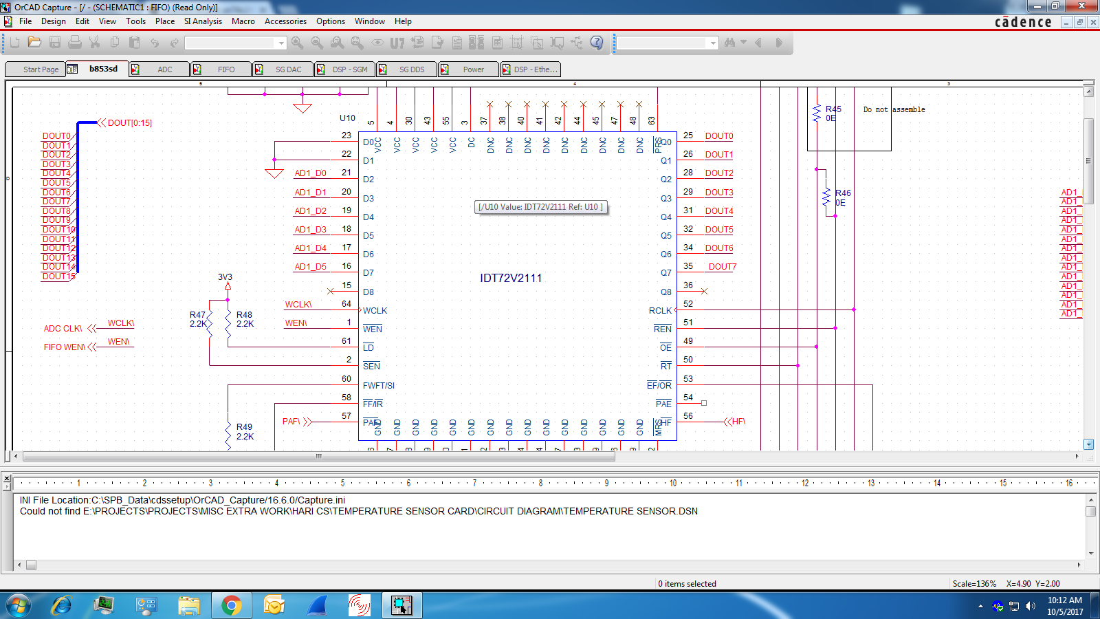
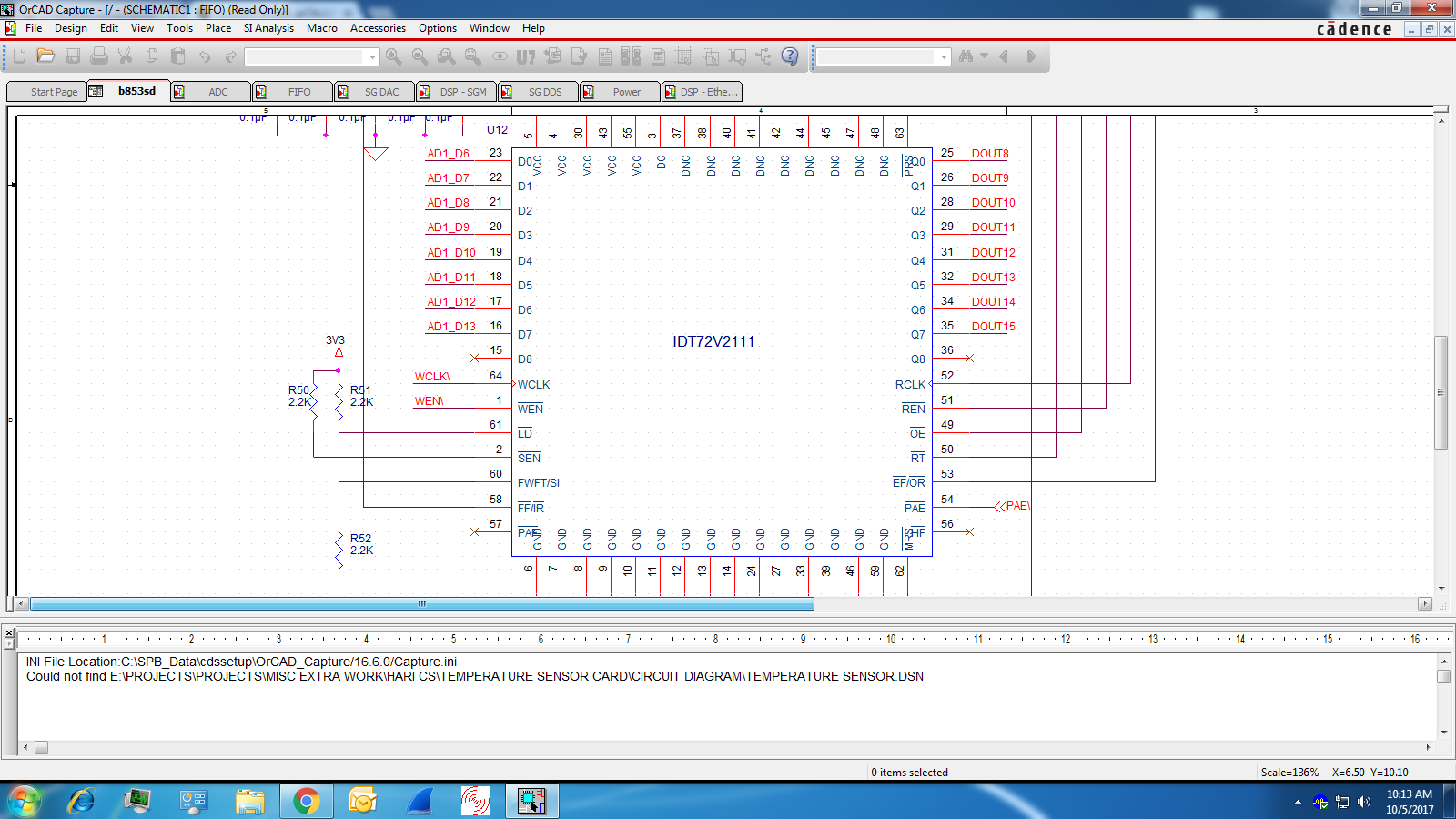
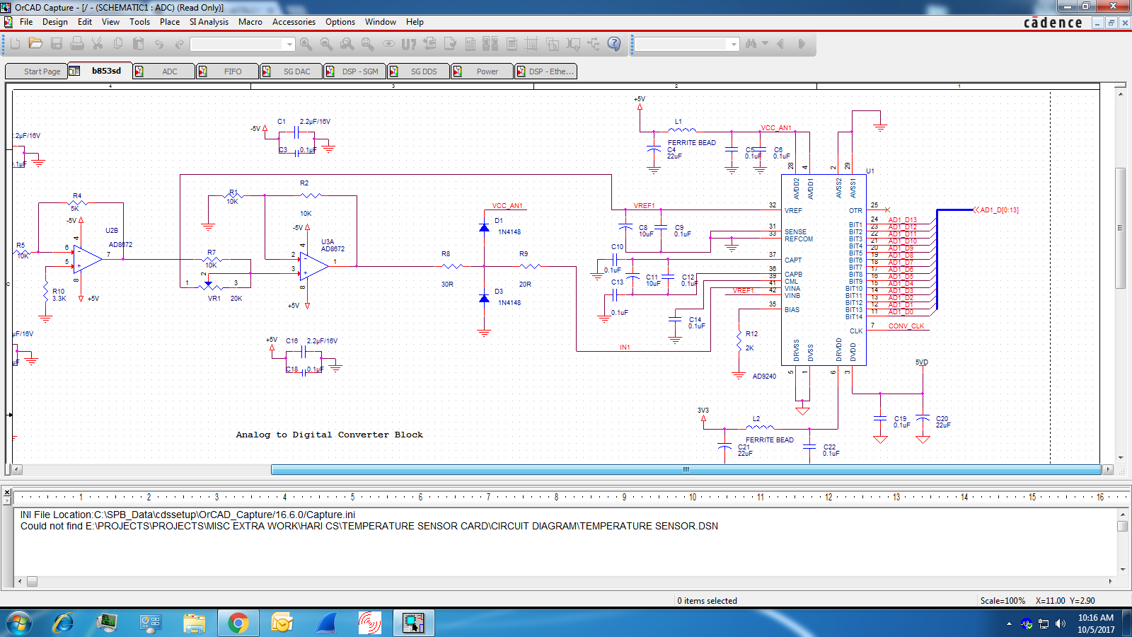
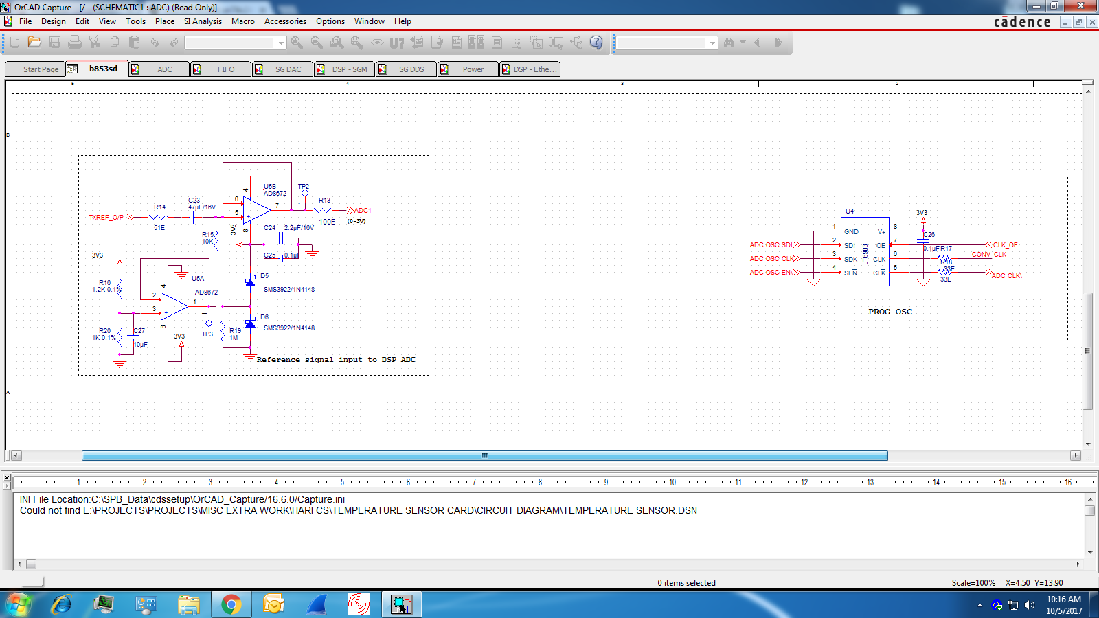
i have generated chirp signal in matlab , there are 1000 samples. now i have to load this signal to fifo and from fifo to dac, i have doubt in loading the signal to fifo. how to code that part?

  • The datasheet contains timing diagrams and requirements to communicate with the FIFO.
    The device (Processor?) that is writing to the FIFO will need to send each word with appropriate timing and mode being used.
    Figure 2 of datasheet shows standard mode word write.
    Regards,
    Wade
  • thank you for the reply, now i have successfully completed write operation , but in the case of reading fifo once a word is read empty flag becomes 0, full flag remains 0 and half full flag becomes one . i have written 4096 samples in fifo . write clk  is given by TMS320F2810. fifo read clock and clock for dac is given by programmble oscillator(ltc 6903) .  following is my fifo read code.

    void Fifo_Read(void)
    {
    GpioDataRegs.GPBDAT.bit.GPIOB15 =1; // enable CLK OE DAC which controls the dac clk & fifo RCLK
    GpioDataRegs.GPBDAT.bit.GPIOB14 = 0; //DAC FIFO OE - to OE pin of fifo(enable OE of fifo)
    asm(" RPT #2 || NOP");
    GpioDataRegs.GPBDAT.bit.GPIOB12 = 0; //DAC FIFO REN - to REN pin of fifo(enable REN of fifo)
    asm(" RPT #2 || NOP");
    while(GpioDataRegs.GPDDAT.bit.GPIOD5 ==1); // DAC FIFO EF
    GpioDataRegs.GPBDAT.bit.GPIOB14 = 1; //(disable OE of fifo)
    GpioDataRegs.GPBDAT.bit.GPIOB12 = 1; //disable REN of fifo
    GpioDataRegs.GPBDAT.bit.GPIOB15 =0; // disable  OE pin of prog osc


    }

  • Shekha,
    Please show oscope plots of the interface. It is not sufficient to debug the FIFO, without seeing the actual signalling and timing.
    Please also provide the schematic.

    It is also critical to indicate the reset sequence.
    The configuration gets set after a combination of events. Look closely at figure 1.
    RS must be high, then transition low for loading the mode.
    There are timing requirements for RS, REN, WEN, LD, and RCLK,WCLK after power up to reset proper mode.
    Can you confirm this is occurring?

    Regards,
    Wade
  • sir,
    can you tell me how to check this timing issues, and how to include these timings in code.
  • i dont know how to upload .jpeg file in this forum
  • fifo is configured in standard mode, single register buffer.partial flag timing mode is asynchronous.
  • To upload an image or file, select "use rich formatting" on lower left of reply dialog.

    Then  use the paper clip to insert a file.

    Regards,

    Wade

  • Thanks for the schematic.
    Do you have any scope shots of the timing for wrting and reading the FIFO?
    Also, confirm the startup reset sequence is performed properly.
    Essentially, need to confirm with scope plots that your GPIO transitions meet the timing requirements in the datasheet.
    Regards,
    Wade
  • sir ,

    now i'm doing sci interfacing of programming oscillator (ltc 6903) , the inputs to sdi, sdk , sen, oe pins are coming from dsp tms320f28335, the respective pins are configured as gpio pins and its direction is set as output. the clock to prog osc is generated by the following code:

    #define ProGOscCLK { GpioDataRegs.GPBDAT.bit.GPIO55 = 0;\
    asm(" RPT #3 || NOP");\
    GpioDataRegs.GPBDAT.bit.GPIO55 = 1;\
    asm(" RPT #3 || NOP");}
    #define CNFbits 0 // CLK : ON, CLK\ : CLK + 180 degree

    problem faced is not getting outputs clk and clk bar.

    regards,

    Shekha Shoukath

  • sir can u please tell how to check whether timing requirements are met using scope plots
  • Sorry, I accidentally deleted this post, and had to have it restored.

    With respect to the programmable oscillator. You will have to check with the vendor that supplies this device to help resolve issues with it. However, I would suggest same methodology. You can probe the interface to make sure that you are providing the programming information as specified.

    For the FIFO, the datasheet has many requirements. The timing diagrams define the order and timing required to properly operate the device. In most cases input timing is defined by required minimums. There are minimum setup and hold times that must be observed. You can take scope plots of signals in question to determine if you are meeting the timing defined in the datasheet.

    Regards,
    Wade
  • sir,

    i probed at Gpio56,55,54 and 53 of tms320f28335. Gpio56 - interfaced to sdi pin of Prog osc, Gpio55 - interfaced to sdk pin of Prog osc , Gpio54 - interfaced to sen pin of Prog osc, Gpio53 - interfaced to OE pin of Prog osc  ( by setting this pin high output clocks- CLK & CLK bar are generated ). as well as @ sdi, sdk,  sen pins of prog oscillator . the scope plots indicates that these pins are functioning as configured. but i didnt get output clocks.

    regards

    Shekha Shoukath

  • Shekha,
    You will need to work with the vendor of the oscillator to debug this.
    I can help with the v245, when you get your clock working.
    Regards,
    Wade
  • hai sir,

    i have two dsps tms320f2810 and tms320f28335. the first one is signal generation dsp and other signal acquisition dsp.

    i have generated a signal using the first dsp, now in the receiver part, the received signal is given to an external adc whose output is given to fifo . these outputs are stored in ram, from there it is sent to pc for monitoring using gui via ethernet. now i connected the transmitter and receiver port via connector but when i run the program and monitor the signal in gui i am not getting the output. can u plz tell me why this happen. 

  • Shekha,
    you are describing a complex system comprising of hardware, software, and firmware. You must debug each part of system to look at expected response and actual response to determine where the issue lies.
    Additionally, it would be more helpful if you posted a pdf version of the schematic. The images above are too low of resolution to see, and not searchable to trace connectivity.
    However, more importantly, you need to determine what of the system is not responding as expected. You can then examine connectivity, timing, software, .... that goes into making that part work properly.
    Regards,
    Wade
  • hai sir,

    is sampling frequency and adc clock refer to the same frequency. i need sampling frequency of 4.5 MHz , does it mean my adc clock should be 4.5MHz?(DSP - TMS320F2835).

    regards

    Shekha  

  • I am not familiar with our competitors ADC, but typically the ADC clock represents the sample frequency.
    Regards,
    Wade