This thread has been locked.

If you have a related question, please click the "Ask a related question" button in the top right corner. The newly created question will be automatically linked to this question.

TLK2711-SP: RX and TX connector placement and differential pair details

Part Number: TLK2711-SP

Hello, 

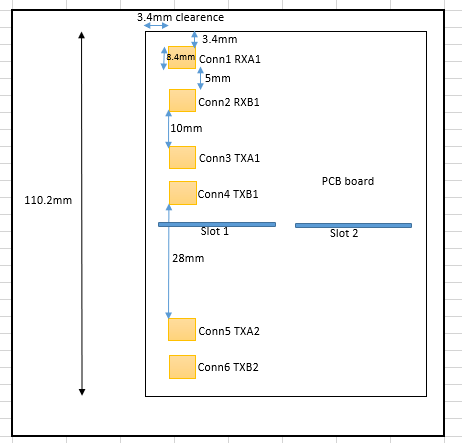
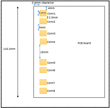
I am designing a PCB which will have 2 TLK2711. The PCB size is limited. So what i need to ask is two things:

1. The input connector placement. I ma using SMA connectors. 8 to be exact on one PCB. I have designed a basic layout, it would be great if someone could verify it, if it would work or not.


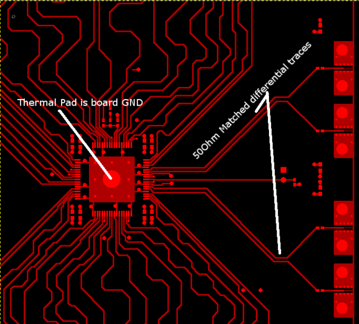
2: Secondly, what I need to ask is, in datasheet its mentioned to make a differential pair 50 Ohm matched. Could anyone please clarify it, either its 2 lines matched at 100 Ohm. i.e one differential pair at 100 Ohm or it is individual tracks matched at 50 Ohm. Which one is it?

Thank you

  • RnD,
    for question number 1, you will need to validate that your placements are routable with selected components and their footprints. It will also depend on if you are using edge launch, or right angle connectors.
    Question 2. This an old question on what is better (or easier to implement). 100 ohm differential, or loosely coupled 50ohm to ground single ended. Most people choose 50ohm to ground single ended that are loosely coupled. That is what is intended on graphic. However, 100ohm differential is good as well, just more restrictive on routing, and will have potentially more impedance mismatches when traces separate for connectors, near device, around obstacles, and if traces needed lengthened for matching other pairs.

    If this answers your question, please click "Verify it as the answer"
    Regards,
    Wade
  • Hi wade,

    Thanks for a quick reply. 

    About the differential lines or 50 Ohm loosely couple lines, if i go as per the graphic, for 50 Ohm loosely coupled lines, do i need to maintain any specific gap between the two transmission lines i.e. one differential pair. 

    Also which one would be better, 4 layer board or 6 layers. One more thing, do i need to give any PCB slots between the two ics'. I mean to avoid any cross talk or to prevent noise migration form IC to IC via ground or power plane. or by any other means.

    As shown below:

    Thanks 

    Regards,

    Bhrugesh

  • Placement query
  • RnD,

    I am not certain the rules, but the routing tool should understand the minimum spacing in order to not influence the 50ohm to ground.   I can research this if you are unable to determine from your layout tool.

    With respect to 4 or 6 layers.  The TLK2711-SP itself can have most if not all signals routed on the top layer.  So needing 6 layers may depend on what other routing resources are required for the board.

    I think I will need more information to comment on whether slots are required for the board.  Are there 2 TLK2711's on the board?  And you are asking if they need isolated from each other?   I think key requirement is adequate filtering for VDDA on each transceiver.  As long as power is clean, slotting should not be required.

    There is a rule of thumb for noise on the power planes for the TLK2711.   VDDA should have less than 40mV of noise, and VDD should have less than 100mV.

    Regards,

    Wade

  • Hello,

    Yes there are 2 TLK2711 IC on board. And yes do they require isolation from each other. So do I have to keep any minimum separation between the TX and RX of one IC to TX and RX of another IC.

    Regards

    Bhrugesh

  • Rule of thumb for spacing for different differential pairs is at least 5x the width of the trace. The pairs should stay on the top of the board (no vias). Best connectors are edge launch.

    I think you can do this in 4 layers, but would be better with 6 layer. Sig, gnd, vdd, vdda, gnd, sig.
    You can split the VDDA plane and filter each from each other.

    Regards,
    Wade