This thread has been locked.

If you have a related question, please click the "Ask a related question" button in the top right corner. The newly created question will be automatically linked to this question.

LP2953QML: LP2953QML

Part Number: LP2953QML

Hello,

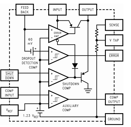
Iam using LP2953QML Die version with Adjustable output option for our designs and could you please clarify whether we can use Noise Reduction capacitor at the REFERENCE pin to the GND to minimize the reference noise.If so what will be the internal resistance at REFERENCE pin to calculate the cutoff frequency.

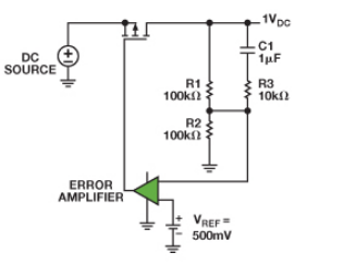
What will be the best optimum value of feed-forward/bypass capacitor across R1 to minimize the error amplifier noise and what will be the maximum value of CFF capacitor we can choose without effecting startup time of the LDO.

What is optimum ratio for R1:R2 to be used for low noise application and Can we use R3 Resistor value in series with feed-forward capacitor to reduce the ac gain of the error amplifier.

Regards,

RVP

  • Hello RVP,

    Unfortunately I do not think we have the internal resistance of the reference pin available. I wouldn't imagine any problem with a ceramic cap on the reference pin though. 

    The optimal value of the bypass capacitor across R1 is found in the section of the datasheet titled Reducing Output Noise. It is Cb = 1 / (2*pi*R1*20). Is this the capacitor you were asking about affecting the startup time? If so, I would imagine staying somewhere near the recommended value (and following the other recommended suggestions in this part of the datasheet) would likely not cause issues with startup time.

    The ratio of R1 to R2 is what sets your output voltage so I'm confused about your question for the optimal ratio. Am I misunderstanding your question? I'm also confused about the circuit you are showing with R3. Where is this schematic found?

    You may also be interested in this TI paper about minimizing noise in LDOs:  

    Thanks,

    Kyle