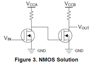
In application report SCEA062A related to 2N7001T. I see some comparations between NMOS level shifter and 2N7001T. When talk about 'Vcc isolation", it says that for NMOS solution, when the power supply is at 0V, the IO pins are not in Hi-Z. I'm a bit confused by this word. Take Figure 3 for example. In my use case, the input source is powered by Vcca, and the receiver logic is powered by Vccb.

- When Vcca = 0, Vin is the input of FET, so the input should be high impedance. The output NMOS's input is pulled to 0V, so the output will output high, as it's pulled to Vccb.
- When Vccb = 0, the input is still high impedance. And the output will always output 0V, right? As the Vccb = 0, the receiver isn't powered, so 0V input is safe in this situation.
So, I can't figure out any problem in this usage with NMOS solution. Can you explain the "Non-Hi-z" problem for NMOS solution more clearly?
Thanks.

