Other Parts Discussed in Thread: SN74AHCT16541
We are using SN74LVCH16T245.

A side connect the power supply +3.3V ,and connect the FPGA output (LVCMOS3.3V).
B side connect the power supply +5V ,and connect the input of ULN2803ADWR.
The direction is A → B.
All OEs are GND. ALL DIR is +3.3V connection.
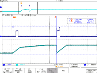
The attached photo shows the waveform on the B side (8 pin) of the SN74LVCH16T245 on the top, and the rising waveform of the +3.3V power supply on the bottom.
It is unclear that the waveform on the output is in the signal of about 2V, probably because the direction changes from B to A until +3.3V rises.
In addition, +5V has started up firster than +3.3V.
Probabily,FPGA signal is in the OPEN state.
Please tell me the reason for this phenomenon.
And please tell me the cause and countermeasures.