This thread has been locked.

If you have a related question, please click the "Ask a related question" button in the top right corner. The newly created question will be automatically linked to this question.

SN74LV4046A: SN74LV4046A : PC2 Average Output voltage vs Input Phase Difference Characteristic

Part Number: SN74LV4046A


Hello,
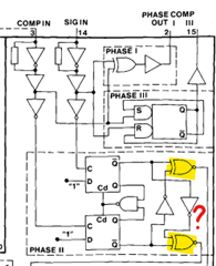
when I compare PC2 Average Output voltage vs Input Phase Difference Characteristic, I obtain with my mockup, to the one in the datasheet,
I have a negative slope instead of a positive slope (while PC1 and PC3 have a positive slope like in the datasheet, so it's not an inversion of the 2 inputs).


Could you explain me why ?

Thank you

  • Bruno, I had thought that perhaps investigating the diagram more thoroughly would produce meaningful results. The diagram of figure three in the 4046 application note (https://www.ti.com/lit/an/scha003b/scha003b.pdf) appears to be nonsensical - even assuming that the reset signal should be continuous high as in the classical NAND-based D-flip-flop implementation, the addition of the XNORs and inverters implies that both NFET and PFET in the charge pump should be active during operation. Clearly these should either be NOR gates or AND gates, instead of XNOR gates. Depending on which gate is actually used, the polarity of the phase detector could easily be inverted.

    I also see a note in the datasheet revision history about changing the x-axis on PC3 output:

    Given the mistakes in the supporting literature, and the already-documented and corrected mistake with the x-axis plot in Figure 8 of the datasheet, I would not be surprised if something got flipped for PC2 and it never got documented.

    In any case, if there is a slope inversion for PC2, you are likely already aware that you can just swap the inputs to get the other polarity.

    Regards,

    Derek Payne