Other Parts Discussed in Thread: SN74HCS595, SN74HC595, SN74LV595A, SN74AHC595, SN54HC164, CD54HC4094, SN54HC595, CD54HC164
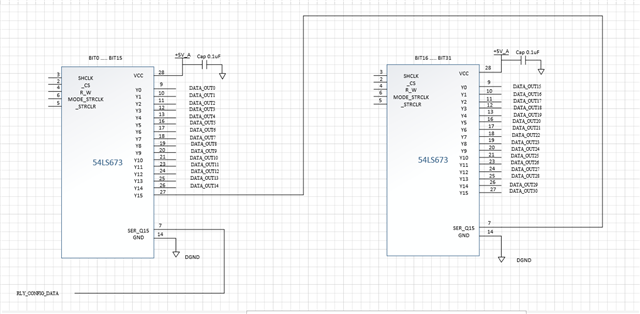
Hi, I am looking to use two (2) SN54LS673 shift registers to process 32 bits of information for my application. The SN54LS673 seems the ideal candidate to perform Serial to Parallel conversion. Shown below in Figure 1 is the basic idea I have for my application. How should I implement two cascading shift registers to count from LSB to MSB? Also, the datasheet does not provide much information about the control inputs and only provides a truth table. Can you please explain how inputs _CS (Pin 2), SHCLK (Pin 3), R_W (Pin 4), _STRCLR (Pin 5), and MODE_STRCLK (Pin 6) work? Can these inputs be shared by Micro GPIO? Please let me know as soon as possible. Thank you.

Figure 1: Serial to Parallel Conversion

