This thread has been locked.

If you have a related question, please click the "Ask a related question" button in the top right corner. The newly created question will be automatically linked to this question.

SN54HC595: 54HC595 8 bit shift register

Part Number: SN54HC595

I am planning on chaining multiple shift registers together to get more states.The data sheet for the P/N #54HC595, (8 bit shift register) has an Qh output and a QH' output. The Qh' output is about a half clock cycle behind the QH signal. To chain two of the 54HC595 shift registers together, I believe I should be sending the Qh signal into the "SER" pin of the following shift register. Can you please let me know if my understanding of combining two 54HC595 shift registers is correct. Thanks Bob Wagner.

  • Hi Bob,

    You will send Qh' from the first shift register to the SER IN of the second shift register. 

    You can refer to this diagram from the HCS595 datasheet: https://www.ti.com/lit/gpn/sn74hcs595

  • HI Albert, thank you for responding. I guess I am surprised at the answer for the 54HC595. So basically you are saying that I should send the delayed signal Qh’ into the next shift register to have 16 bits of storage.

    If I may, I want to compare the similar need of obtaining the 16-bit storage, but with another chip that does not have a half frame delay available, namely the 54HC166 (8-bit parallel load shift register). This chip does not have the delayed output, but rather Qh, similar to the Qh of the 54HC595. So in this case I believe to make a 16 bit register we would send Qh into the SER of the following shift register. So if this is correct for the 54HC166, then why send the delayed in the original case. Now you can see my confusion.

  • Hi Bob,

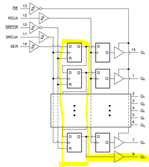
    The Q_H' signal is actually ahead of the Q_H signal -- here's the logic diagram:

    The highlighted DFFs make up the internal shift register, with Q_H' coming directly from the 8th internal register. Q_H comes from the output register, which is going to wait for RCLK to trigger before matching Q_H'. This allows you to shift data through multiple shift registers without changing the outputs until RCLK is pulsed.

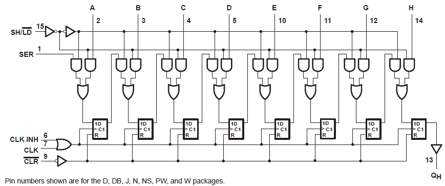
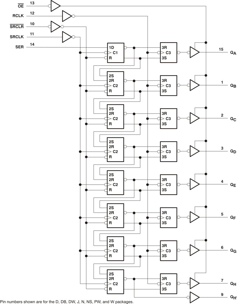
  • With both the '595 and the '166, the pin that outputs the cascaded signal is connected to the last flip-flop of the shift register. On the '595, that pin has a different name because the other pins are connected not to the shift register but to the output register. The pin names are different, but the function is the same.

    '166:

    '595: