This thread has been locked.

If you have a related question, please click the "Ask a related question" button in the top right corner. The newly created question will be automatically linked to this question.

SN74LVC07A: UART Level shifting to & from 3.3V to 5V

Part Number: SN74LVC07A
Other Parts Discussed in Thread: TMP144, , TXU0204

Hello,

I am working on an application where I plan to interface a TMP144 temperature sensor (which operates at 3.3V logic levels & 5kbps baud rate) with a 5V UART logic field bus. I intend to use the SN74LVC07A hex buffer with with 3.3V Vcc & open-drain outputs for level shifting. Power consumption is not a constraint. Here are the key details of the configuration:

  1. Level Shifting from 5V to 3.3V: For the UART Tx line from the 5V field bus to the sensor
  2. Level Shifting from 3.3V to 5V: For the UART Rx line from the sensor to the 5V field bus
  3. Clock Signal Translation: Additionally, using seprate buffer - translating a 4MHz clock signal from 5V to 3.3V logic level for an MCU

The SN74LVC07A is powered at 3.3V, and according to the datasheet, it supports input voltages up to 5.5V, making it suitable for interfacing with the 5V logic levels of the field bus. The datasheet also mentions that both input & output are 5.5V tolerant & the device can be used to translate upto 5.5V or down to VCC.

I have a couple of questions regarding this setup:

  • Is this configuration appropriate for the bidirectional UART communication using two seperate channels as required for interfacing the TMP144 sensor with the 5V bus while the buffer is powered by 3.3V VCC?
  • Can we continue with the assumption based on datasheet that the outputs can be safely pulled up to a voltage higher than VCC ie 5V when powere by 3.3V VCC
  • Are there any additional considerations or potential issues I should be aware of, especially regarding the reliability of the level shifting for the UART communication lines?
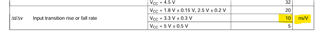
  • Is the idea to use one of the channels for level translating 5V & 4Mhz logic signal into 3.3V signal that can be fed to Clock input of MCU? We will take care of the rise time & the fall times by suitable R-Pull up.

Any insights or recommendations for this type of application would be greatly appreciated.

Thank you!

  • This will work.

    To avoid pulse width distortions of the clock signal due to the slower rising edges of the clock signals, I'd recommend a translator with push/pull outputs like the TXU0204.

  • Hello Clemens,

    Thank you for your feedback!

    I have a question regarding our setup: With trace lengths under 4 inches, is there a risk of significant distortion in the pulse width or rise time of the clock signal? Your experienced perspective would be helpful before we proceed with prototype testing.

    Also, to optimize our Bill of Materials, we're considering using an existing channel of SN74LCV07A rather than installing a new TXU0204 device on the PCB for the clock signal unless it is absolutely required. Do sugget in practicality is this a viable solution in your view?

    Appreciate your prompt feedback.

  • The rise time of the open-drain output depends on the size of the pull-up resistor, so if you can adjust that, then there will be no problem.

  • Hello Clemens,

    I was going through the datasheet of SN74LVC07A & did not find any specifications for rise time, however found the following in the SN74LVC2607.

    So can you guide if we have to assume the same Δt/Δv Input transition rise or fall rate for SN74LVC07A as well or is it more relaxed for '07A device?

    Regards.

  • This specification does not apply; the inputs and outputs are isolated from each other.

    The SN74LVC07A never drives its output high; the output just gets deactivated. So the SN74LVC07A itself has no effect on the rise time.

    The signal is pulled high only through the pull-up resistor, and the voltage reaches the high level after the trace/device capacitances have been charged. In other words, your board forms an R-C low-pass filter.

    You could try to estimate the capacitance as roughly 1 pF per cm of trace, and < 10 pF per device, but in practice, it might be easier to observe the waveform with an oscilloscope.