This thread has been locked.

If you have a related question, please click the "Ask a related question" button in the top right corner. The newly created question will be automatically linked to this question.

TXB0108: how can we use both 8-ch simulation in IBIS model?

Part Number: TXB0108
Other Parts Discussed in Thread: TXU0304,

Hello expert,

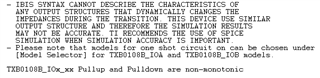
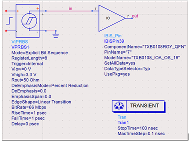
Customer's requirement is 3.3V to 1.8V, B1 is 3.3V and A1 is 1.8V. When they are using ADS simulation, they can only choose single pin which is different from their applicaiton. May we know if we can use all 8-ch simulation here? Thanks a lot!

Best regards,

Ann Lien

  • Hey Ann,

    I have not found a way to simulate all 8 channels at the same time-in my experience, the customer would need to simulate 1 channel at a time with a different IBIS pin each time. 

    You may also refer to the EVM for evaluation of the device under their particular system loading conditions.

    Regards,

    Jack 

  • Hi Jack,

    Thank you for your advice.

    To clarify, does this mean I need to simulate the A & B sides separately? If that's the case, I would also like to confirm whether the input waveform on the A side will affect the output waveform on the B side?

    Best regards,

    Kevin

  • The A and B sides are isolated from each other. But when the TXB detects the beginning of a rising or falling edge of the input signal at any I/O pin, it triggers the one-shot on the other side.

    The IBIS model handles input and output buffers separately, so if your signals actually are bidirectional, then you might need to do two simulations for the same pin.

  • Hi Clemens,

    Thank you for your guidance.

    We are currently conducting simulations for the A and B sides independently. However, I have a follow-up question regarding this setup, specifically related to simulating the round trip delay in ADS.

    For context, here is the SPI topology we are analyzing:
    CPU---TXB0104---COM-HPC conn---COM-HPC conn---TXB0108---conn---TXB0108---MUX---MUX---Flash

    Could you provide any recommendations or best practices on how to simulate the total channel delay time and round trip time in ADS for this configuration to ensure accurate results?

    Thank you in advance for your help.

    Best regards,

    Kevin

  • You must not connect TXB I/Os to each other; a TXB output does not have enough drive strength for a TXB input.

    When using SPI (not QSPI), use translators with buffered I/Os, e.g., TXU0304.

  • Hi Clemens,

    Thanks for your suggestion.

    But I still need to figure out how to simulate the total channel delay time and round trip time in ADS ?

    Could you share how to do it or best practices to ensure accurate results ?

    Best regards,

    Kevin

  • Hey Kevin, 

    You may use transmission line models to model the delay introduced by the cabling/ PCB trace. In any case, we recommend prototyping with the device EVM instead of simulating with the IBIS models since the device is contains one shot circuitry.

    Below snippet is taken from TXB0108 IBIS model:

    Regards,

    Jack