Hello, this is my first time designing a bidirectional application.
SN74LVC16T245 datasheet section 10.1.1 reads:
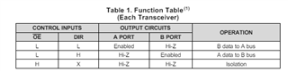
In a bidirectional application, these enable times provide the maximum delay from the time the DIR bit is switched until an output is expected. For example, if the SN74LVC16T245 initially is transmitting from A to B, then the DIR bit is switched; the B port of the device must be disabled before presenting it with an input. After the B port has been disabled, an input signal applied to it appears on the corresponding A port after the specified propagation delay.
This section has me a bit confused.
Does the highlighted section mean that we need to disable SN74LVC16T245 (via the OE pin) and enable it again when we are switching the direction of the buffer?
Also, I have been through the 'switching characteristics' section but I couldn't find a table with the propagation times from DIR to A/B.
Suppose I have SN74LVC16T245 transmitting from A -> B. Now I want to apply an input to the B port. How do I know I can safely apply the input to port B that was previously an output (how long should i wait)?
Thanks in advance,