This thread has been locked.

If you have a related question, please click the "Ask a related question" button in the top right corner. The newly created question will be automatically linked to this question.

TXS0108E: Level Shifter

Part Number: TXS0108E
Other Parts Discussed in Thread: TXB0106

Tool/software:
Dear Team,

Greetings from Dialtronics Systems Pvt Ltd., INDIA.

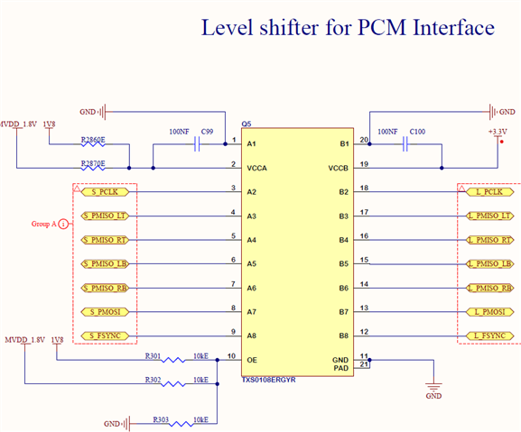
We are using TXS0108ERGYR voltage level shifter from Texas Instruments. 

In the above schematic, we are populating R286, C99, C100. 

Case1: Tried making OE as pull down through 10KE.

Case2: Tried making OE as pull up through 10KE.

In both of the cases we are not getting expected output from the level shifter.

Our Requirement: Input to the level shifter is 3.3V PCM Signals 

Expected output from the level shifter is 1.8V PC Signals.

But we are not getting the expected output.

Input to the Level shifter is fine.

Therefore, requesting you to verify the schematics and share your feedback on this issue.

Thanks & Regards,

Sai Ravali

  • The schematic is incomplete; it does not show the components connected to the I/O pins. Also, how long are the traces?

    See sections 7.3.3 and 7.3.5 of the datasheet for restrictions.

  • Dear Clemens,

    GroupB are the high voltage level 3.3V input to level shifter, GroupA are the expected 1.8V output.

  • Are there any pull-up/-down resistors, capacitors, or other components connected to any of the lines?

    What is the output? Please show an oscilloscope trace.

  • Case1: OE pin made pulled down by 10KE resistor. The expected output is 1.8V PCM Signals. But we didn't get this.

    Case2: OE pin made pulled high by 10KE resistor. The expected output is 1.8V PCM Signals. But we didn't get this.

    Case3: OE pin is made pulled down until VCCA and VCCB are powered up and then made OE pin as pull high once VCCA and VCCB are powered. then also expected output 1.8V PCM signals are not coming.

    Note: Input to the level shifter is 3.3V PCM signals from FPGA the expected output from the level shifter is 1.8V PCM  signals.

    PCLK frequency is 2.048MHz

    Please check the schematics part and suggest if any modifications are required.

    Thanks & Regards,

    Sai Ravali

  • What exactly do you mean with "didn't get this"? What is the output voltage?

  • Dear Sir,

    You can see in the image D18 is the input we are giving to level shifter from FPGA. 

    We are tracing the output at  D4 which is the output from the level shifter which is expected to be 1.8V PCLK signal. But we are not getting any signal.

    We are checking with INTRONIX Logic Analyser in this we cant check voltage level. But atleast we have to get a signal at PCLK which is not appearing.

    Note: operating PCLK frequency is 2.048MHz.

  • I do not know how your logic analyzer is configured. But the line always being low is not a likely error. An oscilloscope trace would be more helpful.

    Please check the TXS's power supply. Try replacing the chip.

  • We are getting 1.8V and 3.3V at the respective pins. Yes, we have replaced the IC. Sir, my doubt is can we use TXS0108ERGYR or TXB0106 (which is 6 channel) for frequency of 2.048MHz? I have seen the datasheet is showing an application circuit output waveforms for 2.5MHz. Still please confirm that can we use TXS0108ERGYR or TXB0106 for operating frequency of 2.048MHz?

  • Yes, they can support 2 MHz.

    But you have not given me all the information I've asked for. Please provide the trace length, or show a photograph of the board.

  • Hi Sai,

    Is the issue only visible on one of the channels or multiple? Are we able to get clarification on Clemens' suggestions of the external loading conditions at the I/Os not shown in the above schematic? 

    Regards,

    Jack 

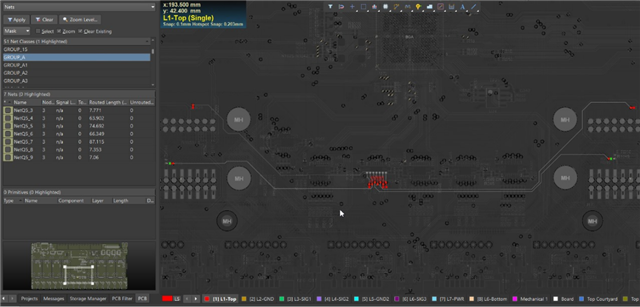
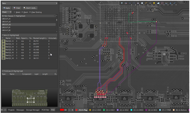
  • Please check the attached Screenshots for trace length.

  • Hi Sai,

    The routing does not seem excessive, though it would be helpful to capture waveforms with oscilloscope instead. Please check for continuity ensuring no shorts and performing functionality test with direct biasing to OE pin to VCCA/ GND without external pullups/pulldowns. 

    Regards,

    Jack