


Other Parts Discussed in Thread: TXU0101, TXU0102
Tool/software:
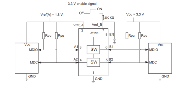
1、It is required to achieve 3.3V to 5V PWM square wave output, using the recommended leakage circuit, FPGA leakage output, 3.3V power supply on the A-side, and 1.5K pull-up resistance; B side is connected to 5.0V power supply, the pull-up resistance is 1.5K, and the EN pin is 200K; The current A side output 3.3V high voltage, B side high voltage is less than 5V, only 4.6V, the current A side output low level, the actual test B side voltage of 4V, the actual test is as follows, yellow, green and blue are respectively B side, EN foot, A side measurement, why do such problems occur?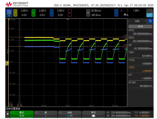
2、It is required to achieve 3.3V to 5V PWM square wave output, using the recommended leakage circuit, FPGA leakage output, 3.3V power supply on the A-side, and 1.5K pull-up resistance; B side is connected to 5.0V power supply, the pull-up resistance is 1.5K, and the EN pin is 0Ω. Measured when the A side is 3.3V PWM square wave, the B side is followed by A high level 3.3V square wave. At this time, the 3.3V supply current of the test A side has a relatively large fluctuation, up to 40mA. If the B side signal can use 3.3V signal, what is the risk of long-term operation?
3、It is required to achieve 3.3V to 5V PWM square wave output. FPGA adopts push-pull output, A side is not connected to pull resistance, directly connected to LSF0108, B side is connected to 5.0V power supply, pull up resistance is 1.5K, when the A side to 100K 3.3V PWM square wave, the test found that the B side can achieve square wave following, but can only maintain more than 20 s, what causes this problem?


