This thread has been locked.

If you have a related question, please click the "Ask a related question" button in the top right corner. The newly created question will be automatically linked to this question.

LSF0108: LSF0108 signals cutting off

Part Number: LSF0108
Other Parts Discussed in Thread: CC3301, TXS0206, TXS0108E

Tool/software:

Hi 

I'm using LSF0108 for SDIO communication between Microchip DSP 3.3V (ATSAMA5D27C-CNR) and Ti WIFI chip 1.8V (CC3301)

See attached Schematics

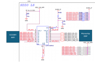
For B side I having PU Resistors of 2.49k

For A side I having NO PU Resistors

Pins 3,10,11,18 are Not in use

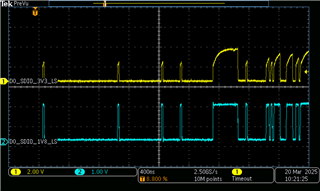
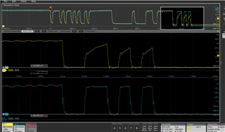
I have measured the CMD and Data signal at I see that during the translation up (meanig 1.8V =>3.3V, from WIFI to DSP) my signal is less square and looks more capacitance 


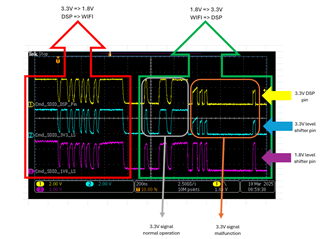
you can see from the pic  above that it  the begging of the translation up the signals looks OK, but after the malfunction start

In this pic I have measured the Do signal:

  • The LSF is a passive switch. After the rising edge of the output has reached 1.8 V, the remaining part of the edge is generated only by the pull-up resistor. Weaker resistors make the edge slower.

    The CC3301 has a specified drive strength of 4 mA, so you can use 3.3 V pull-ups as strong as 825 Ω. Try 1 kΩ.

    The only way to reduce the capacitance would be to reduce the distance between the DSP and the LSF.

  • Hi and thanks for the very quick response.

    We already tried to reduce the PU to 1K but we didn't see any changes - We got the same behavior.

    Also its look that the issue is appeared only in one direction of the communication (From the LSF to the DSP)  the second direction look ok .

    Do you think that PU on the 1.8V side (CC3301) can help to achieve higher drive strength ?

    Can LSFQ can be more suitable for our design ?

  • A PU on the 1.8 V side would not help.

    The -Q1 device works in exactly the same way. 

    Use an SDIO translator like the TXS0206.

  • HI 

    I would like to know what should I do with unused Input/ Output pins:

    1. should I leave them Not Connected? 

    2, This pins have internal PU/ PD Resistor? 

    Please give information for 2 PN:

    1. LSF0108

    2. TXS0108E

    Thank you

  • The TXS has internal pull-up resistors. But even on the LSF, unused pins can be left open.

  • HI ,

    following our investigation we want to have a stronger PU on the 3.3V side to reduce the parasitic RC and provide an higher "High" voltage.

    As expected when reducing the PU value ( Make it stronger) we observe the VIN low is pretty High.

    For example PU of 1K on the 3.3V side provide VIN low ~317mv , and from our calculation its mean that the internal Fet have RDSon of 105Ohm.

    So we thinking that the Fet inside the LSF is in linear mode and not complete open.

    We measured the Vbias across the 0.1u capacitor connected to the Vref B and measured 2.6V .

    We may want to have an higher voltage on vBIAS to ensure the correct operation of the fet and we now want to check to change the 200K Rbias to another value .

    here some question 

    1. Is the analysis sound to you correct ?

    2.The Rbias limi the current flow from the VrefB to VrefA (3.3V to 1.8V) in both cases we are using a TI Buck TPS563208DDCR

    2.1 what is the max current sink that can flow into the TPS563208DDCR ?


  • The circuit with the 200 kΩ resistor automatically regulates the bias voltage to the correct value; no changes are necessary. (2.6 V − 1.8 V = 0.8 V, which is the expected value for the VGS(th) of the internal FETs.)

    The current flowing out of Vref_A is (3.3 V − 2.6 V) / 200 kΩ = 3.5 µA. A buck converter cannot sink any current; if there are not any other 1.8 V devices that consume power and if you observe the 1.8 V supply floating up, add a resistor between Vref_A and GND.

    I recommend the TXS because it has edge accelerators.

  • Hi ,

    Many thanks for the very quick response 

    When measuring the voltage Vin low (from our CC3301 to the LSF and from the LSF to our main MCU) we measured as below 

    * Vout low from the CC3301 is 300mv to the LSF 

    * Vout low from the LSF to our main MCU is 320mv 

    Meaning that only 20mv is the voltage drop on the LSF and its work properly.

    So now the focus is to understand why VOL of the CC3301 is such high (With PU of 1K on 3.3V side)?

    This is mean that internal resistor to GND inside the CC3301 around 80/90 Ohm

  • The CC's output pin must sink the current through all pull-up resistors. With higher pull-up currents, a higher VOL is expected. (The CC3301 datasheet specifies 0.45 V for 4 mA, i.e., 112.5 Ω in the worst case.) As long as it is below the other device's VIL limit, this is no problem.